
 With the continued shrinking of electronic components and the addition of many BGAs to electronic products, it has become more difficult to analyze defects in materials. One common way to do this is through a BGA solder joint section. In this article, we'll do a bit of a primer on this process and how it works in practice.
Solder joint slicing process:
1. Sampling
The test points of the parts to be tested should be clearly marked with a colorful marking so that the sampling is done correctly.
2. Add Glue
Use a ratio of materials and proportion of epoxy resin to hardener of 5:1. The amount mixed is measured according to the number of samples to test. Finally, you would need to record the glue time as the glue must be used within half an hour.
3. Sealing glue
The cut sample should be smoothed with 180# sandpaper with a sand-off of a minimum of 1.27 mm that was reserved for this purpose. Once done, clear with ultrasonic tools.
After this process, the sample should be washed and allowed to dry thoroughly. Once dried, a release agent should be applied to the embedded mold so that the sample can be tested face-down.
A double-sided tape or a sample holder is fixed on the bottom surface of the mold while the clean plastic mold casing is placed on the rotating platform in the vacuum embedding machine.
Once placed, slowly inject the potting material into the embedded mold to ensure that the sample is vertical. After the sample is evacuated in a vacuum embed machine, it can be taken out and allowed to cure at room temperature.
4. Grinding
On the grinding and polishing machine (pictured at right, below), wet the back surface of the circular sandpaper on the surface of the disk, then put the hoop on the hoop to fix the sandpaper.
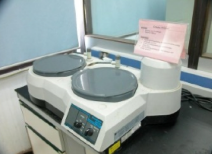
On the sandpaper, the cutting force is rotated at an angle to grind the sample precisely to the position to be inspected. When grinding, it is necessary to flush an appropriate amount of water to avoid the sample until the last wear scar is removed. Once done, rinse the sample with running water and blow dry.
5. Polishing
Polishing must be done until a mirror effect is achieved. It is an important step to obtain the complete slice. The polishing is divided into three steps: rough throwing, fine throwing, and ultra-fine throwing.
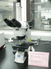
6. Conduct Inspection
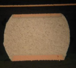
Now, you should be able to confirm whether there are holes or cracks in the joint while observing the tinning degree or coating thickness. The general rule of thumb is that you should try to check at 200 times magnification (or higher) to avoid misjudgment. A sample view of this is shown below.
7. Photography
The intensity of the focal length of the photograph should be adjusted appropriately to give the best image quality. Start the image capture software, capture the image and save the image in an appropriate folder. Now, we have saved our specimen and our solder joint process is complete.
In addition to BGA solder joint cross-sections, surface and internal defect inspection of electronic components can also include coating thickness measurement, PCB and component abnormal condition analysis. These will be discussed in later articles.
Are defects getting in the way of your SMT or PCB/PCBA production?
NexPCB may be able to help.
NexPCB cares about quality production as much as you do.
That is why we are careful to do thorough full inspection on your products before shipping which includes structural reliability and performance testings. Learn more about our quality assurance technologies here.
You can be assured of the quality of your PCB/PCBA and SMT production.
Feel free to tell us your project needs and our team of experienced engineers would be glad to support you!

To learn more about SMT Soldering, technologies, red glue and more, check out the links below:

Liang is a skillful Electronics Engineer with an ability to solder almost anything. By anything, we mean 15+ year old shattered HDD Circuitry to retro gaming consoles .