
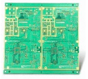
When a printed circuit board (PCB) is fabricated, the overall size of the full board will be much larger than the final product board. In most cases, multiple "copies" of the PCB are made on a single, larger piece of material before they are cut into the size of the final board. In may ways, the way that these boards are cobbled together is like a puzzle that is a balance of efficiency of the fabrication process as well as optimization of subsequent processes that create the final product.
For the PCB design, hardware designers will generally consider electrical signals and the arrangement of the components on the final board with a specific focus on functional issues of the product. Designers don't generally think as much about the considerations around manufacturing and assembly of the final PCB. The best results for the final product will balance between function and manufacturability. When an SMT process is required for final assembly, special attention needs to be given to the PCB layout to optimize speed of placement of the components. To gain the best optimization, arranging the "puzzle" is also very important.
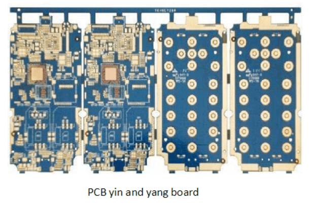
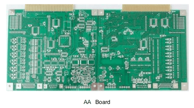
The examples above show some boards that have intentionally not been separated so as to keep them as a larger unit. This improves the efficiency of the SMT placement because there is less transition time between boards and the equipment can be run at higher utilization. The higher the utilization of the equipment, the quicker the final product can emerge.
The Decision Process of the Puzzle
The main decision points around how to put this puzzle together revolves around the capabilities and attributes of the SMT equipment as well as some specifics of the board:
-
The process capability of the equipment
-
The maximum size of the board that an SMT system can handle will place a limit on how many attached PCB's can be routed at the same time.
-
The number of boards that can fit within this maximum size will also play a role as the board size may not evenly divide into the size of the SMT maximum.
-
The number of components that can be loaded into each process stage will also be important as more components will require more reels be loaded into the system and affect efficiency.
-
-
PCB thickness
-
The thickness of the board will directly affect the performance as the board size increases.
-
If the board is thin, then there is a chance of deformation during the reflow stage of the SMT process if the board(s) are too large.
-
-
Production operation complexity
-
The design characteristics of the board may make the production process complex.
-
For example, if the board is very thin and the size is large, it can be more fragile and easily damaged during the process.
-
How to Keep the Puzzle Together
Between the internal veneers of the separate puzzle pieces (final PCB's), there still needs to be a connection between the pieces that maintains some structural strength of a single part while making the parts easy to separate once the assembly processes are complete. Some considerations been to be made so as not to create follow-on quality issues. The two main types of connection methods are :
-
V-cut
This is a V-shaped groove that is mitered into the board at the boundary between two separate circuit boards. This is generally done with a very fine drill that is precisely drawn across the boards (pictured below)
-
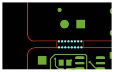
Perforations
Similar to tear lines in paper forms or the edges of a postage stamp, this method drills tiny holes in a straight line at the demarkation boundary between two separate circuit boards. These holes can be as small as 0.5mm or 1mm. This is pictured below from a PCB layout (the cyan dots) :
In either case, the purpose of dividing these puzzle pieces is the meet the efficiency requirements of the SMT process. After assembly is completed, the boards must be separated to finish the single-board assembly. The design of the panels should consider both the larger board assembly requirements as well as the sub-board after production. Balancing these requirements can yield a high quality product that is also efficient to manufacture.
If you have any questions about this process or need someone to help you with layouts that are designed for high volume manufacturing, we're here to help! We have layout services available for any complexity. If you can't find any packages that suit your needs, don't hesitate to contact us!

Liang is a skillful Electronics Engineer with an ability to solder almost anything. By anything, we mean 15+ year old shattered HDD Circuitry to retro gaming consoles .