
Care should be taken to distinguish between single ended and differential trace impedance. High speed single ended signals such as the parallel RGB LCD or camera interface need to be routed with the specified single ended impedance. This is the impedance between the trace and the reference ground.
High speed differential pair signals such as PCIe, SATA, USB, HDMI etc. need to be routed with differential impedance. This is the impedance between the two signal traces of a pair. As the signals are also referenced to ground, each differential pair signal also has a single ended impedance. When selecting trace geometry, priority should be given to matching the differential impedance over the single ended impedance. The differential impedance is always smaller than twice the single ended impedance

The signals allow a certain impedance tolerance (e.g. 50Ω ±15%). When defining trace geometry, try to keep the calculated impedance value as close as possible to the exact impedance value. This allows greater flexibility during PCB manufacturing. Variation in impedances will occur between different production lots. If the calculated impedance is in the middle of the tolerance band, this will help ensure maximum production yield.
Different tools can be used for calculating the trace impedance. Polar Instruments offer a widely used tool. Many PCB manufacturers use this tool. PCB manufacturers can often help customers with impedance calculations, and it is suggested you work with your chosen PCB manufacturer during your design. Many PCB layout tools offer a very basic impedance calculator. Unfortunately, these calculators are not reliable in all situations.
Traces on the top or bottom layer have only one reference plane. These traces are called microstrip. The following figure shows the geometry of such microstrips. H1 is the distance from the trace to the according reference plane. Er1 is the relative permittivity of the isolation material. The traces have a trapezoid form due to the etching process. In the layout tool, the traces have to be designed with a width of W1. W2 depends on the trace height (T1) and the duration of the etching. Contact your PCB manufacturer in order to get the information about the resulting width W2. S1 is the spacing within a differential pair.


Traces in the inner layer of a PCB have two reference planes, reducing electromagnetic emissions and increasing immunity to external noise sources. These traces are called stripline. The following figure shows the geometry of such striplines. When making impedance calculation of striplines, special care needs to be taken when it comes to the isolation thickness H1 and H2. H1 is the thickness of the core material. The traces are embedded in the pre-preg material. As the traces have a finite height, the pre-preg height H2 depends on the copper density. The relative permittivity of the core and pre-preg material can be slightly different. Many impedance calculation tools can take this in account.
If you want to now more about Relative Permitivity, here is a comprehensive article detailing the process.


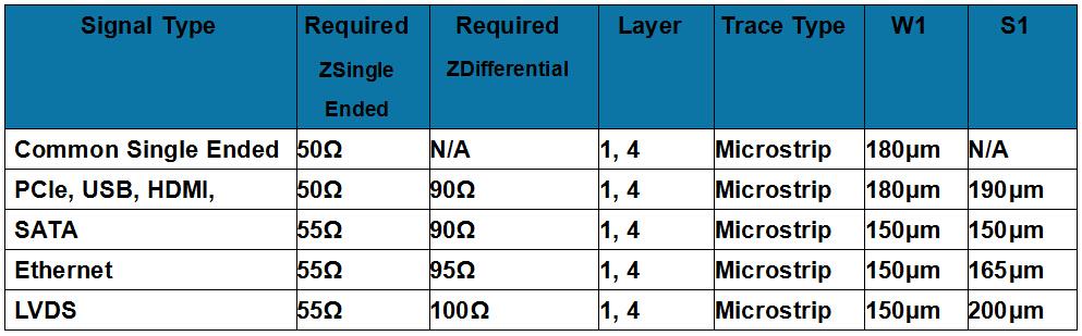
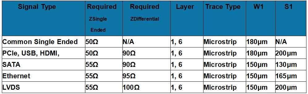
The following table shows typical trace geometries for traces using in the six layer stack-up,
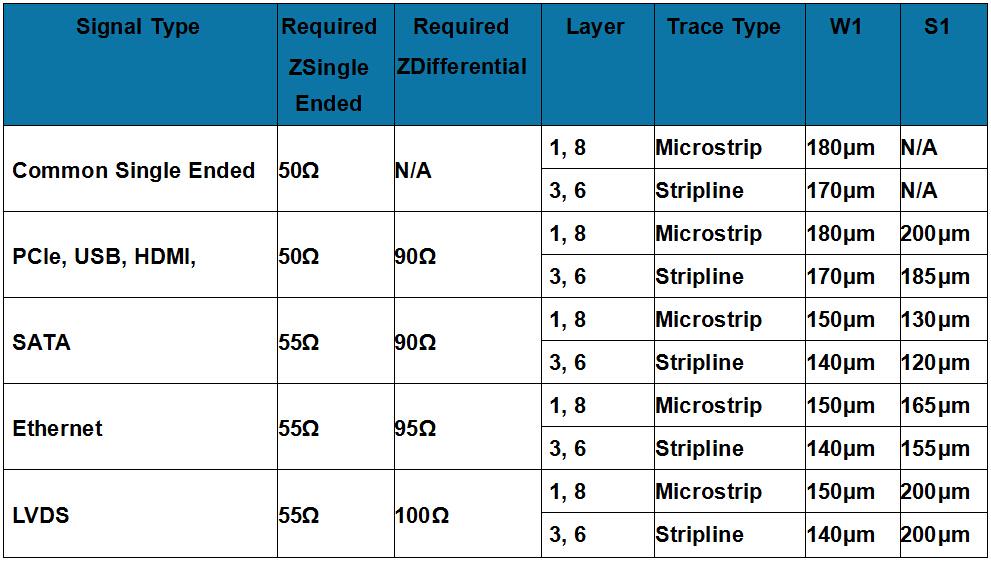
The following table shows typical trace geometries for traces used in the eight layer stack-up,

Anything that was written as a group effort is added here. One for all, all for one!