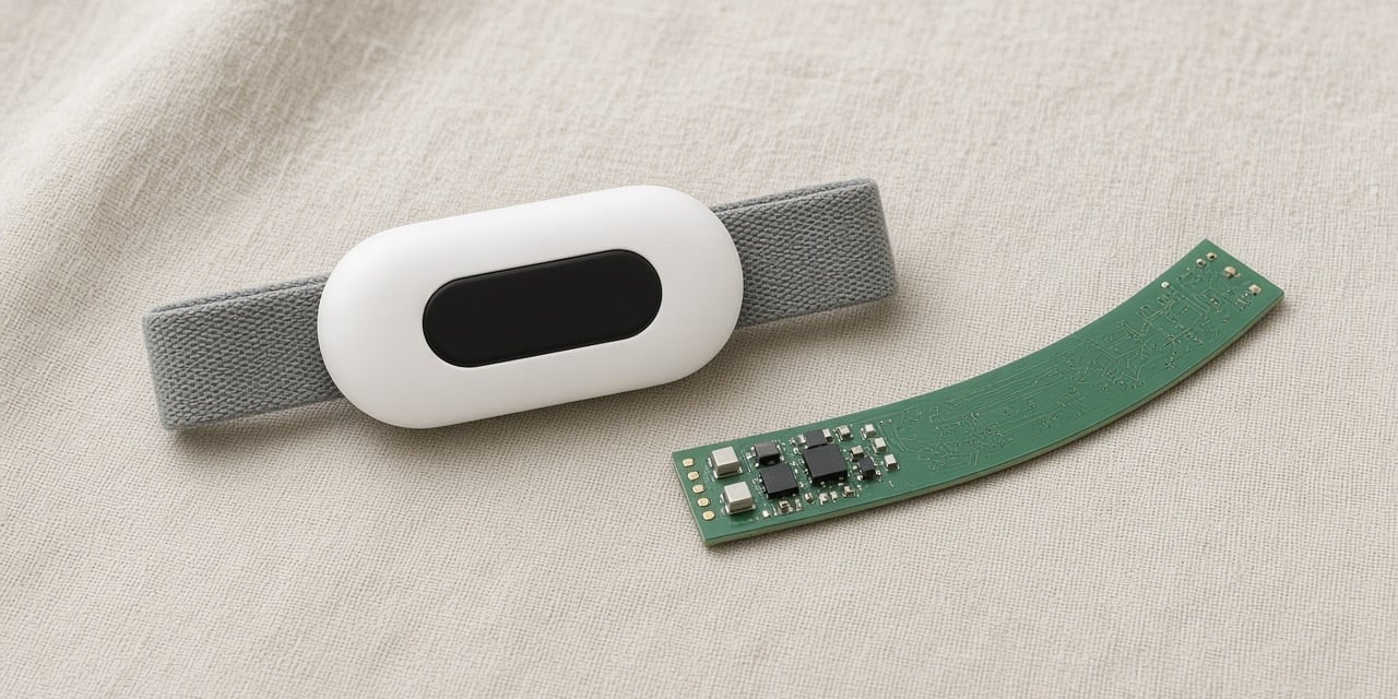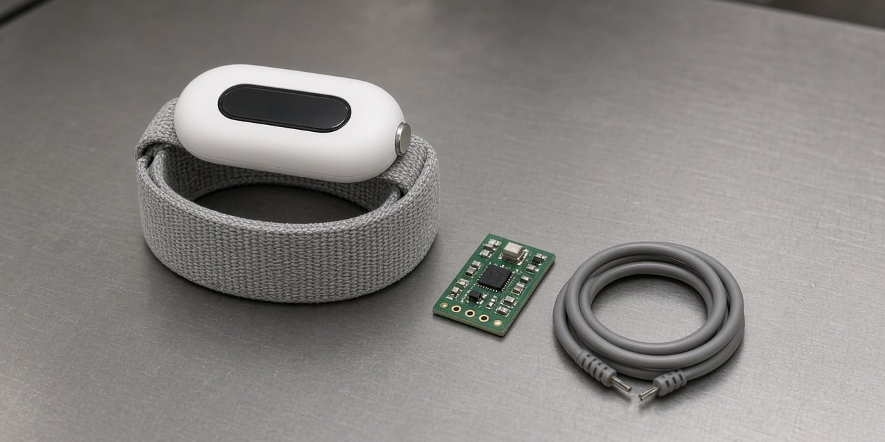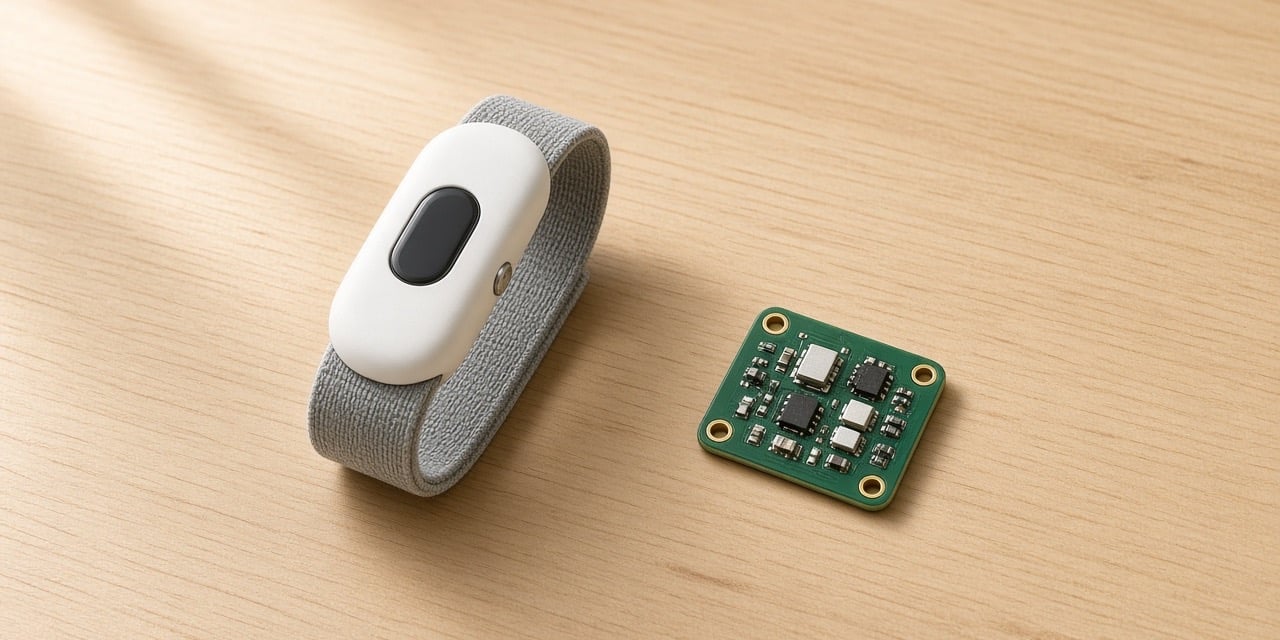
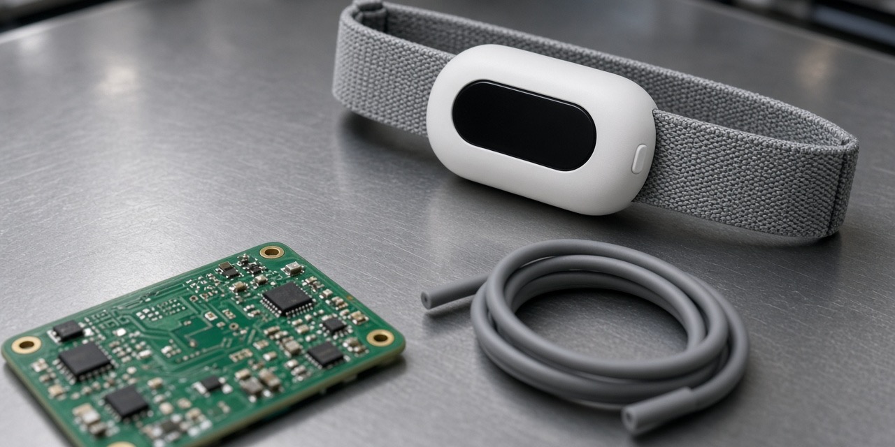
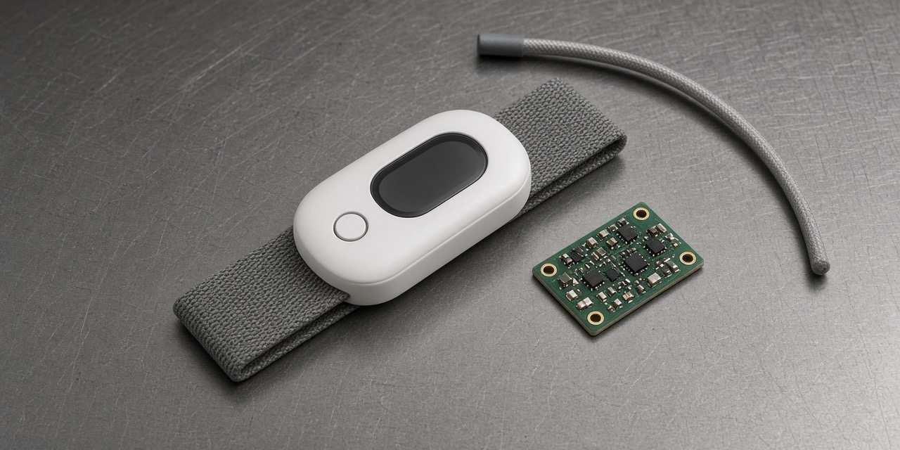
Power, the clock, the driver, and the interface are one order for thinking through a bring-up. Wearable firmware and hardware integration at NexPCB can start there. A later failure is not unreadable only because an earlier step was skipped. The pins and registers come with the hardware file. The cable in the photograph is a concept of a programming lead. It is not an SWD lead already connected.
What firmware and hardware integration checks first
Before the bring-up, the hardware file says which of those four the build will confirm, and which pins or registers are provided for each. One useful order is the rails, then the clock, then the driver, then the timing. It is not the only order.
| Step | What you provide | What power-up has to show |
|---|---|---|
| Power | The voltage each rail requires, and the test point | Each rail is inside its window, in the right order |
| Clock | The crystal specification and where start-up is checked for the clock that should be running | That clock source has started, in the enable state the file names. A crystal that is not enabled at power-up is not required to be running |
| Driver | Register differences and the configuration the part expects | The identity register reads the expected value, and the configuration bits are written |
| Interface | The debug pins and the firmware files | The debug port connects, the image checks, and the peripherals start without an error |
What firmware integration needs for power and the clock
On a camera module the analog rail, the digital core, and the IO rail were 2.8 V, 1.2 V, and 1.8 V, and the first pin on the connector was power. On a module bring-up the list walked the power-management outputs, including 0.8 V and 1.8 V, and the rails the module itself made for its peripherals. The check after power-up on those boards is the same one: each rail that should be up is inside its window, in the order that was written.
The clock file names the crystal and the point where start-up is checked, for the clock source that should be running. On that module bring-up a scope confirmed the main crystal had started and the waveform was the expected shape, and a second crystal on the power-management circuit was checked as well. A camera module carried a 24 MHz crystal. A ring program kept its 32 MHz main crystal. A crystal that is held disabled is checked in that disabled state. It is not required to be oscillating at power-up.
What you provide for the driver and the interface
The driver file includes the register differences of a substitute. On one SPI flash, two part-number suffixes differed in the QE bit of the status register. That difference belongs to that flash, and it matters when Quad mode is used. The bit defaults to zero and can be programmed, and the firmware writes it when this build uses that mode. The same bit is not a rule for every SPI part. That default is part of the hardware file for that flash. On an image sensor, the correction table had to be the confirmed values. A readback once showed the defaults instead, and the version register read all zeros. On an I2C converter the log reported an init error. That log line is the error that was reported. It does not by itself mean the I2C port never came up. After power-up, the identity or version register is read against the expected value, and the configuration bits are checked against the ones that were written.
The interface file names the debug and programming pins, and it includes the firmware files. On a watch, the Gerber and the schematic were used to confirm the SWD pins: SWO, SWCLK, SWDIO, reset, and ground. The client for this project released the code early so programming could be prepared. On a dual-core BLE controller the network core was write-protected, and a full erase with the wrong file left that protection in place. The right network-core file and the right application file wrote normally on that log. That result stays with that chip and that log. After programming, a readback checked the image against the partition layout. The cable photograph does not show that connection.
Frequently asked questions
Can the driver be debugged before the rails are confirmed?
The rails are a useful first check. A driver error can still be read when an earlier step was skipped. The cause is then looked for in the step that failed and in the steps around it.
Who writes a register bit that defaults to the wrong value?
On the SPI flash whose suffixes differed in the QE bit, the firmware writes that bit when Quad mode is used. The hardware file for that flash says so before bring-up. The difference belongs to that flash.
What to bring before power-up
Bring the rail voltages and the test points, the crystal each clock that should be running uses, the register bits a substitute does not default, and the debug pinout with the firmware files. Name the check each step has to show after power-up. Start at our project inquiry form.