NTI Acceleration Program

New Technology Introduction
 
Particular focus on the critical phases of
prototyping and pilot runs, while driving
significant enhancements to EVT, DVT, and PVT processes.
Accelerate My Project
nexpcb-nsf-framework

Experienced engineers with knowledge covering almost all the IoT product technical stacks, decades experiences in the electronic R&D and manufacturing industry.

DFM checks to mitigate potential risks prior sending to production, saving the waste of producing defects product

Qualified PCBA production covering almost all the complexity, with high quality deliveries, and tests.

Reports created since the beginning of project and the end of delivery, to continuously improving your next stage

Cost down suggestions Supply chain management,  risk evaluation, BOM optimization. As a result you will get a final business analysis report.

half-of-customers-startups
Our customers are startups, or
organizations seeking reliable, trustful and
consistent support through early stage
development, NPIs and lifecycle
management capabilities.

Consulting

We understand the critical importance of this stage towards to the success of launching New Product to the market(NPI), which is in our team’s DNA.

Experts from engineering, supply chain and management, is capable of supporting you through your early stage design to the end of product life cycle.

Talk to the team
  • Strategic consensus
  • IP Security
  • Technical excellence
  • Expert Evaluation
  • Quality Standards
  • Certifications
  • Supply Chain
  • Cost Planning

Support on your design phase

Schematic

Schematic

Our engineers is able to support your design review and provide know-how experiences.

Layout

Layout

Reliable layout service. It ensures signal integrity, power integrity, and electromagnetic compatibility.

PCB fabrication

PCB fabrication

Up to 68 layers, with Min Traces/Space at 3 mil. Microvia-based any layer HDI PCB. 

PCB assembly

PCB assembly

Covers soldering methods like reflow and wave soldering, precise connections for components such as BGAs with tiny 0.3mm/0.4mm ball size. 

Test & debug

Test & debug

Execute tests, root cause analysis and repair before delivery to reduce time from fixing issues. 

IPC
ISO
RoHS-1
UL
component-sourcing.webp

Component Sourcing

Layout

pcb layout

* The lead time is calculated from the number of pins, roughly 400 pins per day and 3 days for creating footprints. For instance, 2000 pins design, the layout time is approximately 8 business days. 


Max. Layers

64

Max. # of Pins

150000+

Max. connections

120+

Min. Trace Width

2.4mil

Min. Spacing

2.4mil

Min. Through Holes

6 mil (4 mil micro-via)

Max. # of BGA

120+

Min. BGA Pin Spacing

0.3mm

Max. BGA Pins

8371

Max. High Speed Signals

112G-PAM4


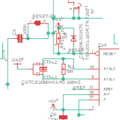
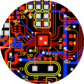
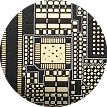
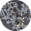
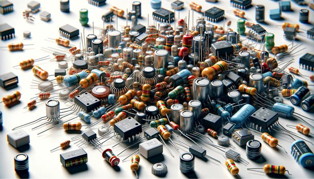
PCBA fast prototype in 3.5 weeks

In 2 business days

. RFQ
. TECHNICAL REVIEW
. QUOTE

In 3.5 weeks

. PAYMENT
. PROCUREMENT & PRODUCTION
. TEST & DEBUG
. DELIVERY

Technical Review

DFx


Production files

Gerber file*

Drill file*

BOM*

Pick & Place*

ODB++ 

(required for design checks)


Original design files

Schematics

PCB Layout


Response time:

Within 2 business days


DFM Report (optional)

Standard PCBs

Rigid


Layers: 

Up to 24 layers


Board thickness:

584mm x 508mm


Min. Trace/spacing: 

3 mil


Copper weights:

1/3oz, 0.5oz, 1oz, 2oz, 3oz


Materials:

FR-4, Mid-TG FR-4, High-TG FR-4, Halogen Free, Aluminum, Rogers


Surface finishes:

ENIG, HASL, HASL-Lead free, IAg, Immersion Tin, OSP,  Gold Fingers


Lead time: 

2-12 layers: 5 - 12 days

> 12 layers: contact us

Advanced PCBs

Rigid, Flex & Rigid-Flex, HDI


Layers: 

Up to 68 layers


Board thickness:

550mm x 900mm


Min. Trace/spacing: 

2 mil


Copper weights:

1/3oz, 0.5oz, 1oz, 2oz, 3oz


Materials:

FR-4, Mid-TG FR-4, High-TG FR-4, Halogen Free, Aluminum, Rogers


Surface finishes:

ENIG, HASL, HASL-lead free, IAg, Immersion Tin, OSP, Edge Connector, ENEPIG


HDI PCBs supports max 28 layers, with Any layer complexity, the minimum microvia size at 3mil.  

PCB Assembly

Min. component size:

0.4mm x 0.2mm


Max. component size:

120mm x 90mm, or 150mm x 25mm


Min. BGA pitch: 

10mil (0.25mm)


Testing:

AIO min. 15μm

SPI and X-ray


Lead time:

Start from 1 day


Depanelize::

V-Cut

Table-Route

Component Purchase

Lead time:

Start from 1 day, as normally 2-3 weeks.


Preferred distributors:

Digikey, Mouser, Avnet, Future, Pulse, Wurth, Holder, Coilcraft


Global component search with our networks.

Test & Debug

Provide testing instructions or firmware if needed. Our engineers can make the  toolkits and execute tests and generate reports.


We are also capable of assisting diagnosing issues.