In the process of the PCBA production, there are several common problems may occur including tin beads, inscription, bridging, virtual welding, ointment collapse, weld point dimming, and situations where residue is obvious and dark in color. In this article, we will specifically look at the issues of insufficient and excess solder.
What are the insufficient solder and excess solder?
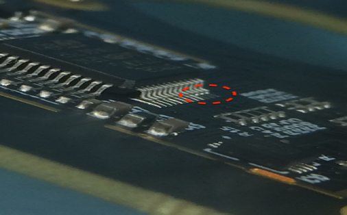
For an insufficient solder condition, it means the tin is not enough in the solder points when the board is initially tinned. This situation could cause virtual welding and poor connections in the circuits. The following figure is an illustration of this situation on an actual board.
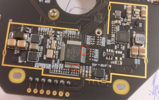
For the situation where there is excess solder, it means, conversely, that there is too much solder applied during tinning. If the assembly is tight, it can affect the assembly, the packaging, the amount of tin and the coverage of the solder joints. The following figure is shows the situation on an actual board :
In the all, the amount of the tin for the PCBA is a significant factor in the quality of the production and life of the product.
What is the standard of tin?
The acceptable standard of the tin is summarized with a few points :
- The tin point should be smooth.
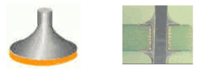
- The connections should be shiny and totally wetted with the welded parts.
- The contour of the components should be easy to distinguish.
- The solder joints of the soldered areas should have smooth, concave edges.
- The through holes should be completely filled with tin.
- The tin points should be well polished.
What is the solution of the above two problems?
1. Insufficient solder
This requires agreement with the SMT provider to execute 100% AOI and x-ray confirmation for BGA packaged chips. This provides confirmation of the quality on a regular basis. At the same time, key inspection for shipments is also needed. At NexPCB, we check whether the corresponding IC's have exposed pads as part of our normal QC (see below).
2. Excess solder
This is also an operation in agreement with the SMT provider. The will need to properly clean the PCBA after the patching work is completed. The cleaning of the packaging
.png)


.png)