A System In a Package (SIP) is a functional package that integrates multiple functional chips, including processors and memory, into a single package that achieves a completely functional system unit. This can sometimes be confused with a System-on-Chip (SoC) package, but the difference is that the SIP is a side-by-side or superimposed package with different chips while the SoC is a highly integrated chip product. SIP can more simply be defined as a combination of multiple active electronic components with different functions with optional passive devices. These can also include other devices such as MEMS or optical devices, so the SIP can achieve a certain function of a single standard package. From the perspective of package development, SIP can be considered a basis for SOC package implementation.
SIP package form
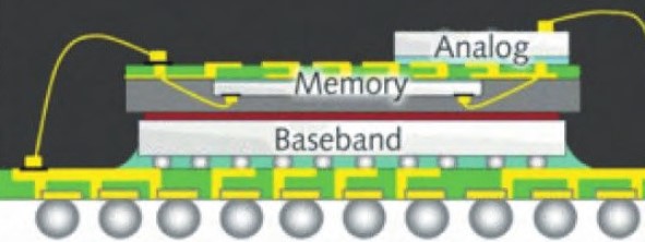
The SIP technology accepts many types of bare chips and modules for arrangement and assembly. These can be structured in either a planar arrangement (2D) or in a stacked arrangement (3D). The 3D packaging method, specifically, allows for more modules to be used in a smaller space and makes the overall functional integration more appealing. Internally, the components can be bonded using wire bonding, flip-chip, or a combination of the two.
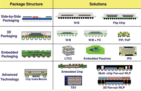
In addition to the 2D and 3D package structure, it is also possible to use a multi-functional substrate to integrate components where the different components are built in the multi-function substrate to achieve the purpose of functional integration. Different chip arrangements, combined with different internal bonding technologies, enable a variety of combinations of SIP packages and can be customized or flexibly produced according to a customer or product requirements.
The technical difficulties of SIP
The most common packaging method for SIP is using ball grid array (BGA) technology, but there are complexities with using this or any other packaging method. From a circuit design perspective, the 3D chip packaging will have multiple die stacks, so this creates complications in how to layout the packaging. For example, multi-chip integration into a single package must account for spacing between traces, complex trace patterns, potential interference between devices, clock signal frequency differences, and many considerations about the physical size of each separate device. When doing these designs, considerations about such arrangements, once taken, will be simulated with complex software to ensure system performance. This is key since the actual process of fabrication is complex and the design should be well understood before proceeding.
SIP packaging technology market prospects
Compared to system integration on printed circuit boards, SIP maximizes system performance, eliminates re-packaging, shortens development cycles, reduces costs, and increases integration. Compared with SoC, SIP also has the characteristics of high flexibility, high integration, short design cycle, low development cost, and easy access.
The SIP package integrates other components such as passive components and antennas into a single package for a more complete system function. From the point of view of application products, SIP is more suitable for low-cost, small-area, high-frequency and high-speed, and short-lived electronic products, especially power amplifiers (PA), global positioning systems, Bluetooth, portable product markets such as image sensing module and memory cards. These characteristics also make these products highly applicable to industrial applications, Internet of Things, mobile phones and smartwatches. There are also very broad markets in the fields of smart bracelets and smart glasses.
At present, when intelligent hardware manufacturers design smart wearable devices, the main challenge is how to put all the required functions into a very small space. Taking smart glasses as an example, in the hardware design phase, it is necessary to consider the characteristics and integration methods of main components such as wireless communication, an application processor, storage memory, photographic lens, micro-projection display, sensor, microphone, etc., while also evaluating component integration. The use of the SIP system miniaturization design can simplify system design is key for meeting their design criteria. It can increase the portability of the product while adding a lot more functions without changing the appearance.
At present, the global output of packaging capacity alocated to these types of packaging accounts for only 10% of the total value of integrated circuits, but the emergence of SIP is likely to break the current industrial structure of integrated circuits since changing the package is only a issue at the subsequent processing plant. In the future integrated circuit industry, there may be a group of entities that combine design capabilities and packaging processes that maximize value of their products and profits of their own brands. When the SIP technology is mastered by a packaging company, the output value of the packaging industry has significant potential moving forward.
.png)


.png)