With the mass production of electronic products, the method of manual welding is no longer appropriate for market requirements, production efficiency, and product quality. Hence, manual immersion tin and semi-automatic/fully automatic welding equipment have been developed. We will step through this process in this article.
After the completion of wave crest welding and spray flux process, the PCB plate is transferred to the preheating zone. The solvent in the flux is evaporated while the rosin and active agent in the flux begin to decompose and activate. Oxidation film and other contaminants are removed from PCB pads, component ends, and pin surfaces. In the meantime, the PCB and components get fully preheated.
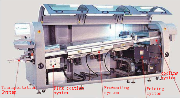
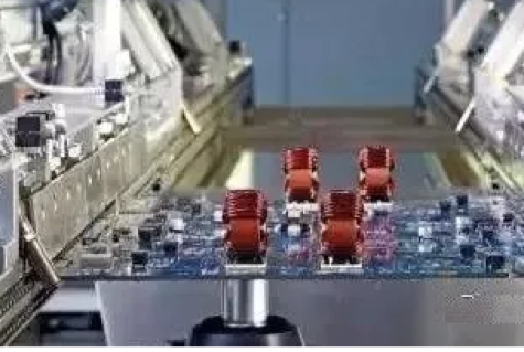
The PCB circuit board continues to move forward. The bottom of the board will initially pass the first molten solder wave. The first solder wave is the random wave that will print the welding flux to all the solder plates, the component solder end, and the pin of the bottom of the printed plate. The molten solder will infiltrate and diffuse over the surface of the metal that has been cleaned by the flux. After that, the bottom of the board will pass through the second molten solder wave. The second wave is a smooth wave, which separates the connecting bridge between the pin and the welding end and removes welding defects such as drawing tips.
With enhanced awareness of environmental protection, new welding technology has been developed. The tin-lead alloys were used in the old days, but lead, as a heavy metal which is harmful to the human body, has fallen out of favor as part of the process. Hence, lead-free technology has been created to ensure better health. These newer processes use tin-silver and copper alloy with special flux. The required temperature for welding and preheating is higher, and a cooling zone is needed when PCB boards pass through the welding area.
Eutectic solder is also excellent in electrical conductivity, stability, corrosion resistance, tensile strength, mechanical strength and technological performance with abundant resources and low prices.
.png)
.png)
.png)
.png)