Having been working with startups from more than 50 countries around the world, we have started seeing a pattern in the initial design-related problems companies face when launching hardware products. From product design to prototyping, and all the way to mass production processes, there are some key areas where you too may be facing similar issues.
Today we'll be talking about three of the most common design errors we receive from startups working with us.
1. Defective Soldering Due To Deformation of Pads
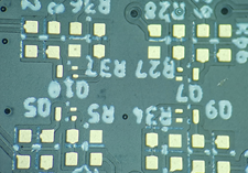
As you will see in the following pictures, we had a situation in which a pin on several SOTs (small outline transistors) had deviated from the other one with the same size, and some irregular deformations were present. These kinds of pad shrinkage or small deformation will lead to insufficient soldering. The asymmetry between the pin legs also increases the chances of pseudo soldering (i.e., looks soldered, but in fact isn't) or the drifting of components occurring. In such cases, we usually suspect if the designed footprint is wrong. However, the design files showed no mistakes. The designed SOT dimension was of a SOT23 soldering pad standard.
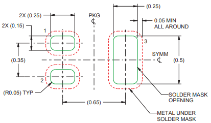 Minimum Pad Layout Dimension in mm
Problem:
The presence of any acute or right-angle corners in wiring tracks is usually avoided in PCB design, as these sharp corners may lead to the formation of “acid traps” (breakage due to excessive corrosion of the copper layer). The sharp corner tends to accumulate the chemicals, creating a pool of acid at the tip of the tracks which corrodes the soldering pad. The condition shown in the pictures below describes the problem, as shown by the presence of the tracks' sharp angular design. The trace of the pin is very thin, and the track width is equal to the soldering pad width.
Solution:
If wider wiring is applicable, it is recommended to make the end width of the wiring larger than the soldering pad by about 1.5 times. This solution reduced the chances for ‘acid traps’, similar to the copper etching process. For T-connections, a "teardrop" connection must also be made. With these design improvements, the probability of ‘acid traps’ from occurring can be effectively reduced.
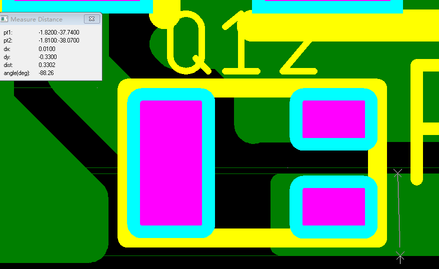
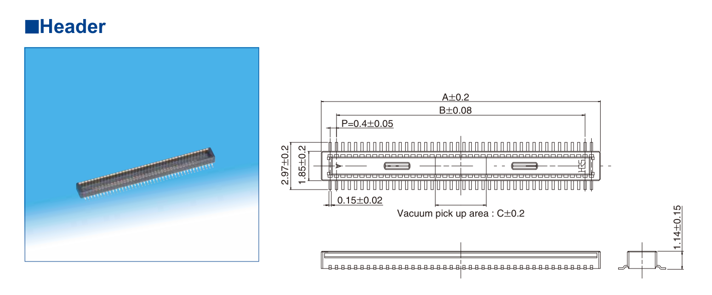
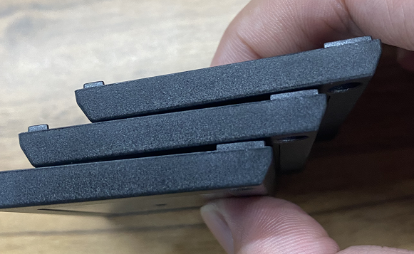
2. Shifting of Bilateral Symmetric 4BTB Connectors
Boards with symmetrical BTB connectors like the one in Raspberry Pi CM4 Module have now become a more common design. However, during the mass production process, there's a chance that at least one of the connectors will bend. Some of the tilted products might not be observable with AOI and to the naked eyes, but problems could be detected when adaptation tests are conducted. These problems include over tightness, difficulty in plugging, or poor contact after repeated use.
Problem:
The four headers are symmetrical to each other and require a very high positioning accuracy (i.e., narrow tolerance) in order to support connections between the board and its peripheral devices. We know that each of the components itself has its own tolerances. During the heating process in the reflow oven, a natural shifting process will occur, because there's molten solder moving around, and the magnitude of this shift isn't always included in the designed tolerances. This, however, means that the tolerances should consider the shifting process that could occur in both positive and negative directions. If the shifts of the three headers are in the same direction, but the shift of only one header is going in the other direction, a tolerance overlap will occur, leading to the plugging difficulty of one of the headers.
Solution:
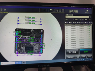
First, the part was tested. The mounting precision test was done to check whether the part passes the two testing steps. The first one is done by using a high-precision testing fixture to screen the products with tilted components. The second step is to use the optical comparator with the precision of 0.003mm to test the products with suspected problems screened in the first step again for the second time.
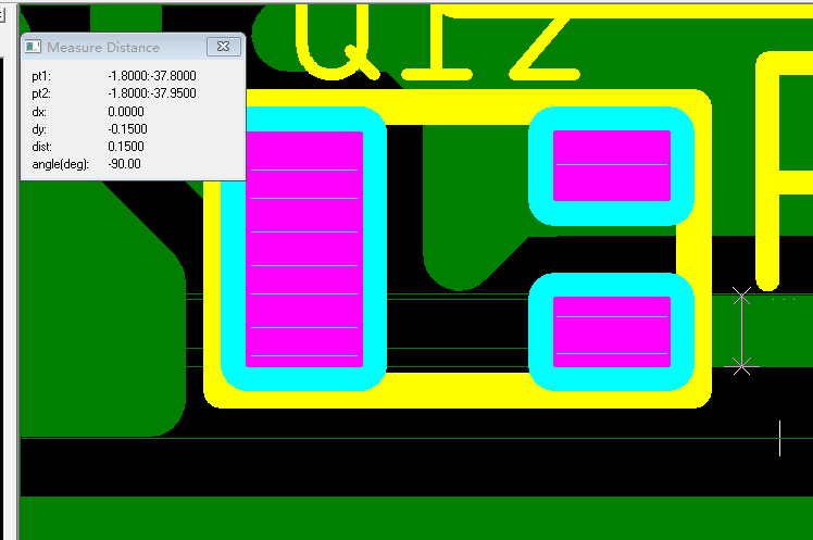
After the product passes the test, we can say that the products are qualified, but we still need to solve the tolerance issues in design or manufacturing and assembly processes. We know that there are three grades of pad design according to the IPC standard, namely low density, normal and high density. For scenarios with strict tolerance requirements, we generally recommend designing the pads as high-density soldering pads, to solve the problem by the basis of designing with a very small size. This way, the drifting of the components in the reflow oven will be minimized. The design of the 4 headers' soldering pads is then modified to reflect the changes.
Finishing Process:
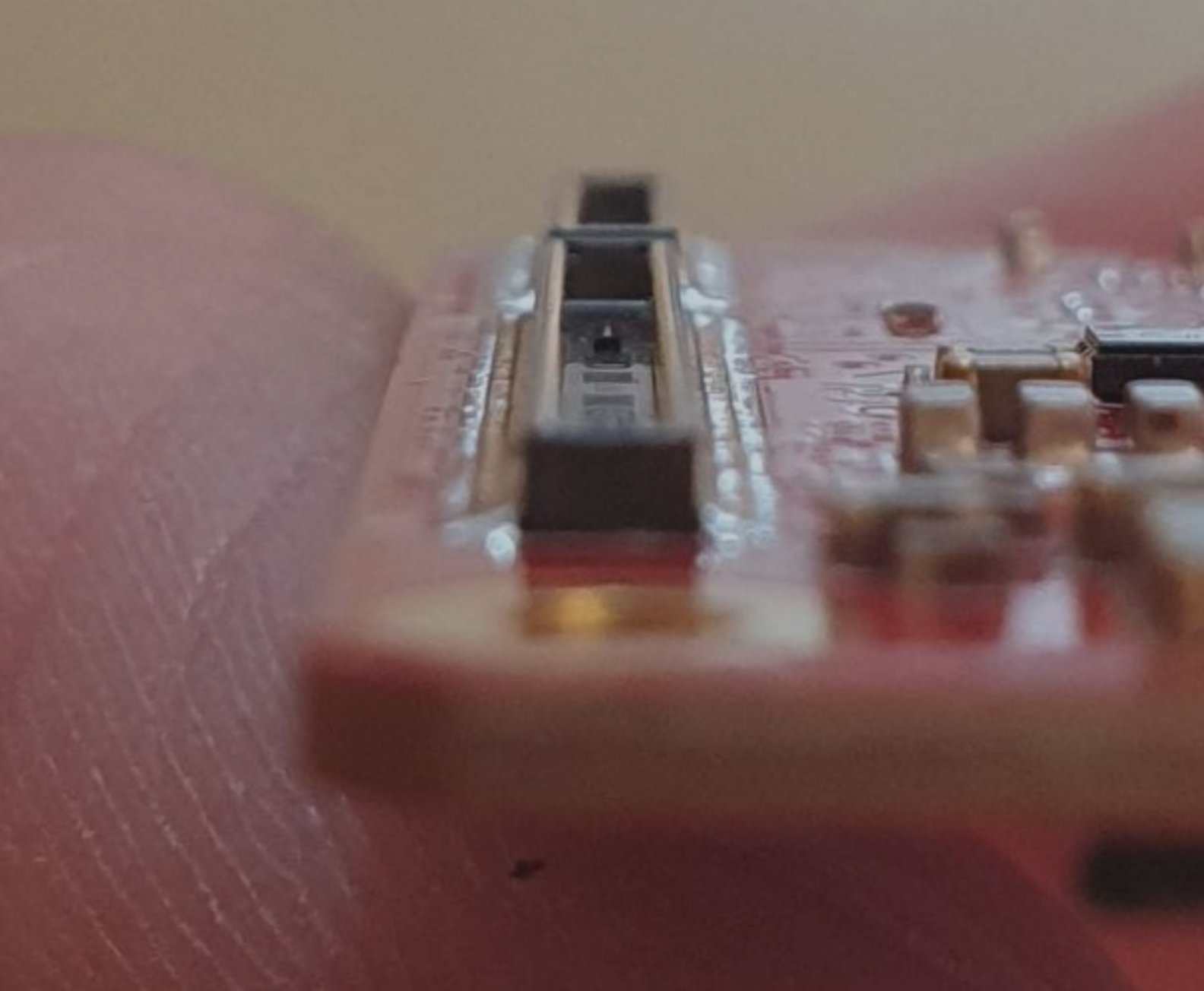
Sometimes, even with the high-density pad design, a certain degree of shifting still occurs. In cases like this, the problem might be caused by the mounting process. NexPCB has designed a special suction nozzle shown in the following picture for this purpose, which has the same length as the connectors to minimize the displacement caused by movement or vibration during mounting, to reduce the funky results we may sometimes have for which we blame the laws of physics for.

With the above measures, we can control the relative precision error of the four interfaces to be within 0.05mm.
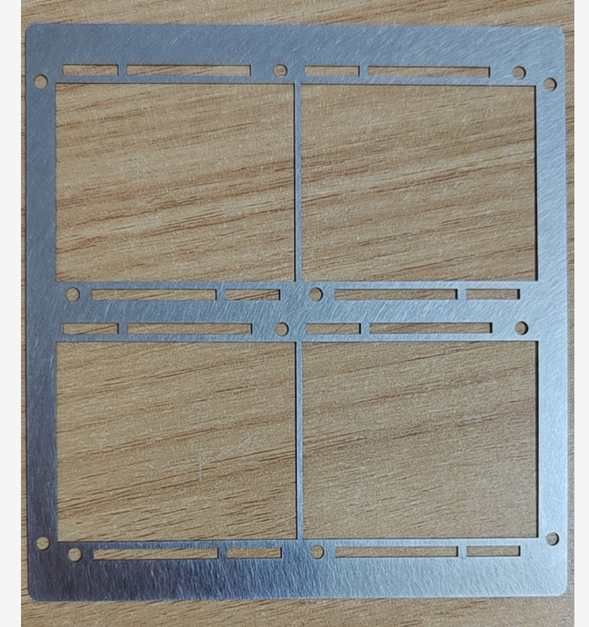
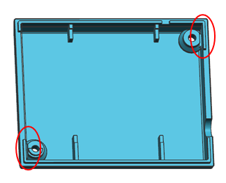
3. Depression of Plastic Housing
During the injection molding process of a product’s plastic housings, it is highly probable that the outer walls at the screw holes may shrink inward, forming depression points shown in the following picture. Improving the qualification rate of the injection machine through commissioning is very hard. This may lead to a serious problem for mass production and supply.

Problem:
After reviewing the design drawings, we found that the screw boss position was merged with the outer wall, making the thickness of this position much higher than that of the frame. During the cooling process of injection molding, the contrast between cooling speeds and stresses led to the inward shrinkage of the material, causing depression.

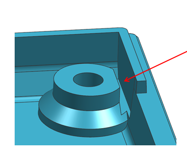
Solution:
To solve this problem, we first go further into the initial product design file. In the design file, the screw boss was then designed to be separated from the frame of the housing. After altering the mold, all depressions were eliminated, and the failure rate of mass production was minimized immediately.
These are just a few of the DFM issues we solve every day. Although these problems are likely more common than you think, with a solid manufacturing partner like us (wink wink), it's easy to overcome them.
.png)


.png)