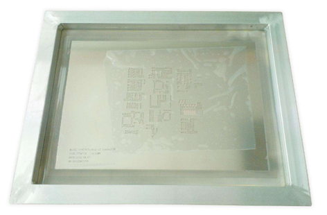
SMT steel mesh, which is used to consistently distribute solder paste or patch glue, is the outer tool for ensuring the quality of printing solder paste and patch red glue. In the electronics industry, SMT surface mount is a very mature process technology. Maturity, however, does not always mean defect-free. On the contrary, with the further miniaturization of electronic component packaging, process problems are particularly prominent and more difficult to control. The technology used in the solder paste printing process is related to the success or failure of SMT soldering. The design and manufacture of steel mesh
1. Description of steel mesh
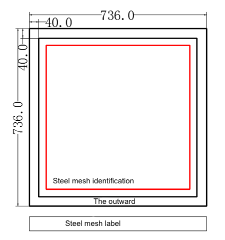
1. The outer frame of frame steel is 736*736 mm with a precision of 0/-5 mm. The mesh frame thickness is 40*40M with a precision of 0/-5mm. The steel sheet is 590*590mm with a precision at +/-10mm.
2. The center of PCB, the center of steel sheet and the center of the outer frame of the steel grid need to be overlapping where the maximum distance between the three centers should not exceed the mesh. The mesh direction should also be consistent so that the two lines' angular deviation is not more than 2°
3. The surface of steel mesh must be free from deformation, dirt, and oxidation.
4. The pad openings also must free of deviation. Of important note here is that the number and position of openings must match. The openings need to be free of deformation with no burr (i.e. smooth texture).
5. The reference MARK is sintered on the lower surface at a distance of at least 3 points with a diameter of 1 +/-0.15MM
6. The peripheral and central tension shall not be less than 45N/cm;
2. Steel mesh engraving methods
There are a few different methods for engraving the mesh parts. Below are 3 and their overall comparisons.
| Method | Advantages | Disadvantages | Applicability |
| Etching |
Low Cost |
Poor opening configurations Rough hole walls Limited size |
PIN >0.65mm QFOP Devices |
| Laser Engraving |
High Precision |
High Cost Burring on interior hole walls Requires Chemical Polish |
Pin ~ 0.5mm BGA and QFP devices |
| Electric Casting | High Precision Consistent Openings Smooth interior wall holes |
Expensive process Longer time to completion |
0201 Materials <0.3mm QFP devices |
.png)


.png)