1. The role of MARK
The "mark point" is also called the reference point and is the point of positioning when the SMT machine is used. Because PCB products provide common measurable points for all steps in the assembly process in mass production, each device used in the assembly can accurately position the circuit pattern for precision. These marks allow for the machine to be automatically set by the programmer after the program is loaded. The Mark point is the primary calibration point, so the MARK point is critical to SMT production.
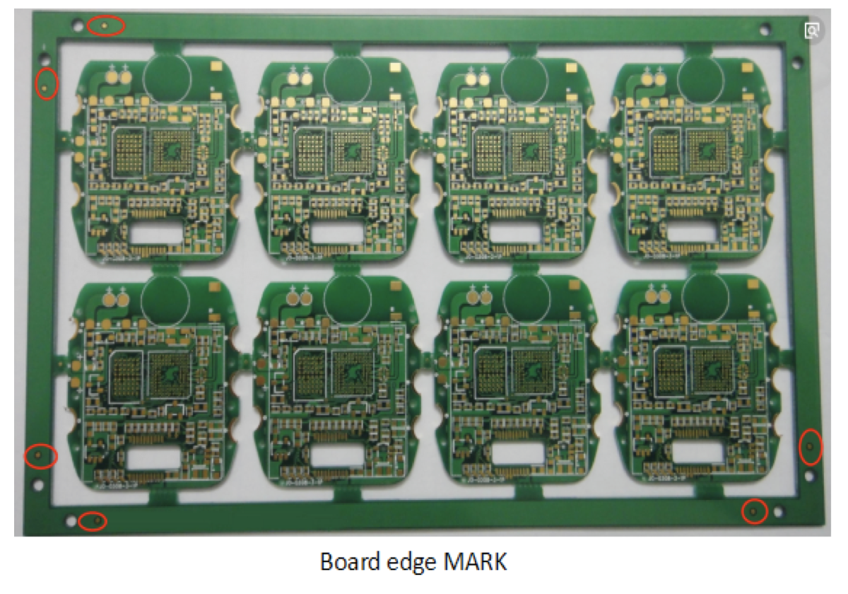
2. Mark point design specifications
The Mark point is marked as a solid circle in the photo below. Each PCB board must have at least one pair of mark points that can meet the design requirements for SMT machine recognition and must have a single board
The PCB Mark has a minimum diameter of 1.0 mm and a maximum diameter of 3.0 mm. All mark points on the same board PCB must be the same size. The mark point (edge) must be ≥ 5.0 mm from the edge of the printed board (the minimum spacing required for the machine clamp PCB) and must be within the PCB board rather than the edge of the board and meet the minimum mark point space requirement. If you're not sure about this, ask your PCBA provider to let you know what these tolerances are.
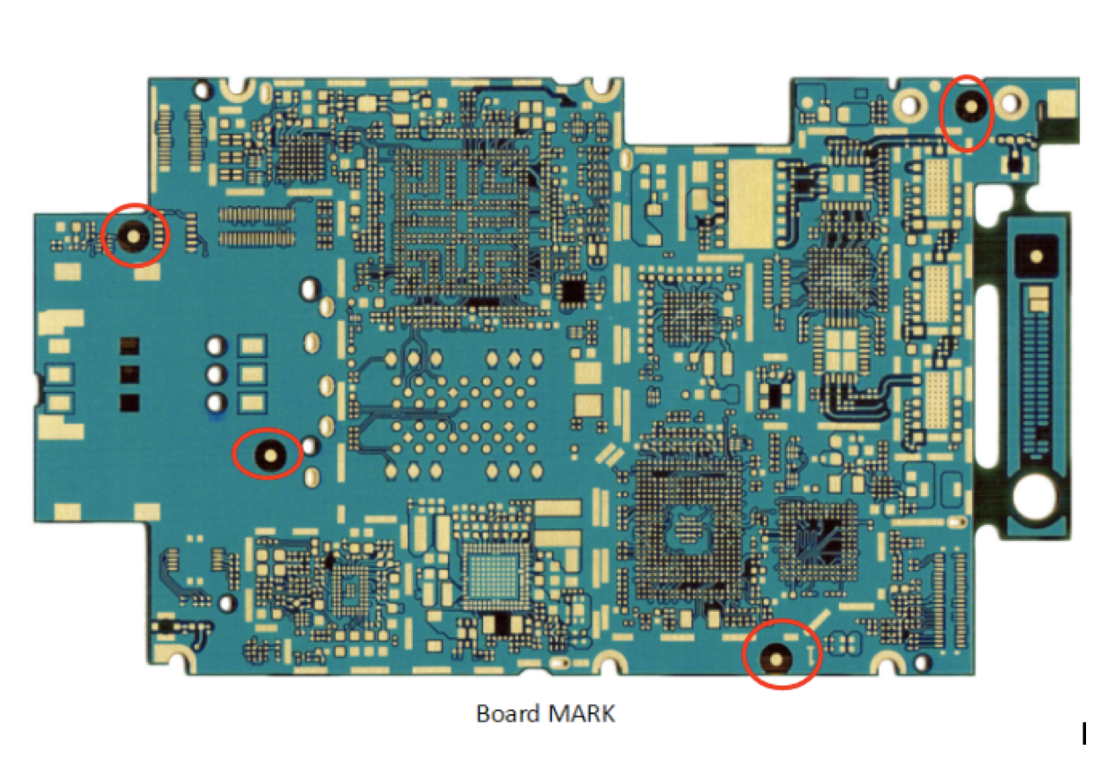
3. The shape and design specifications of the mark point
1. The marking point used to position the placement machine is actually a special layer of the pad, which is usually placed on the opposite side of the PCB for machine identification. The mark points on the PCB are generally designed with round, square, triangular, diamond, or another identifiable shape. The main shape of these can be identified by the SMT machines so the board can be positioned in the machine correctly.
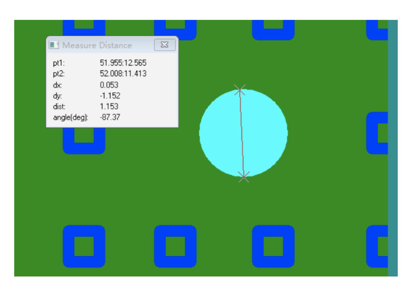
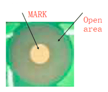
2. The suggested mark diameter is R = 1.0MM (solid circle), composed of a complete mark point including marked points and open areas.
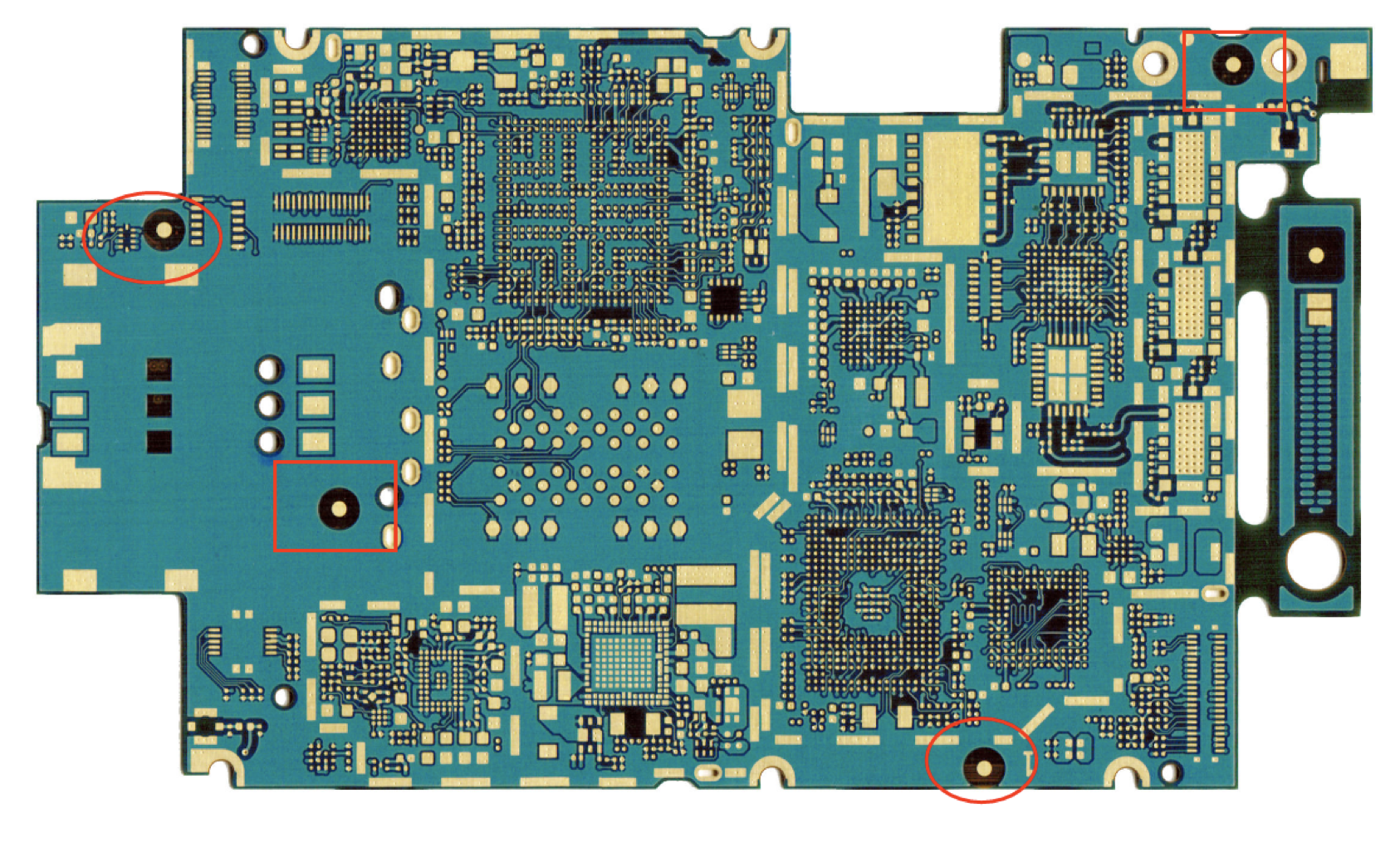
3. When the PCB is assembled, the relative position of the mark point of each board must be the same. The position of the mark point on any board on the board cannot be moved for any reason and the position of the mark point of each board should be asymmetrical.
4. All mark points on the PCB are only satisfactory when the two MARK points appear on the same diagonal and in pairs, which plays the role of machine positioning recognition. This is why the mark points must appear in pairs in order to be effective.
NexPCB offers full layout services for your project if you're unsure how to make this all work together. Our team of layout engineers
.png)


.png)