The design of IoT PCBs plays an important role in the ever-evolving world of IoT, where wireless communication is crucial. At the heart of this lies Radio Frequency (RF) design and signal integrity management.
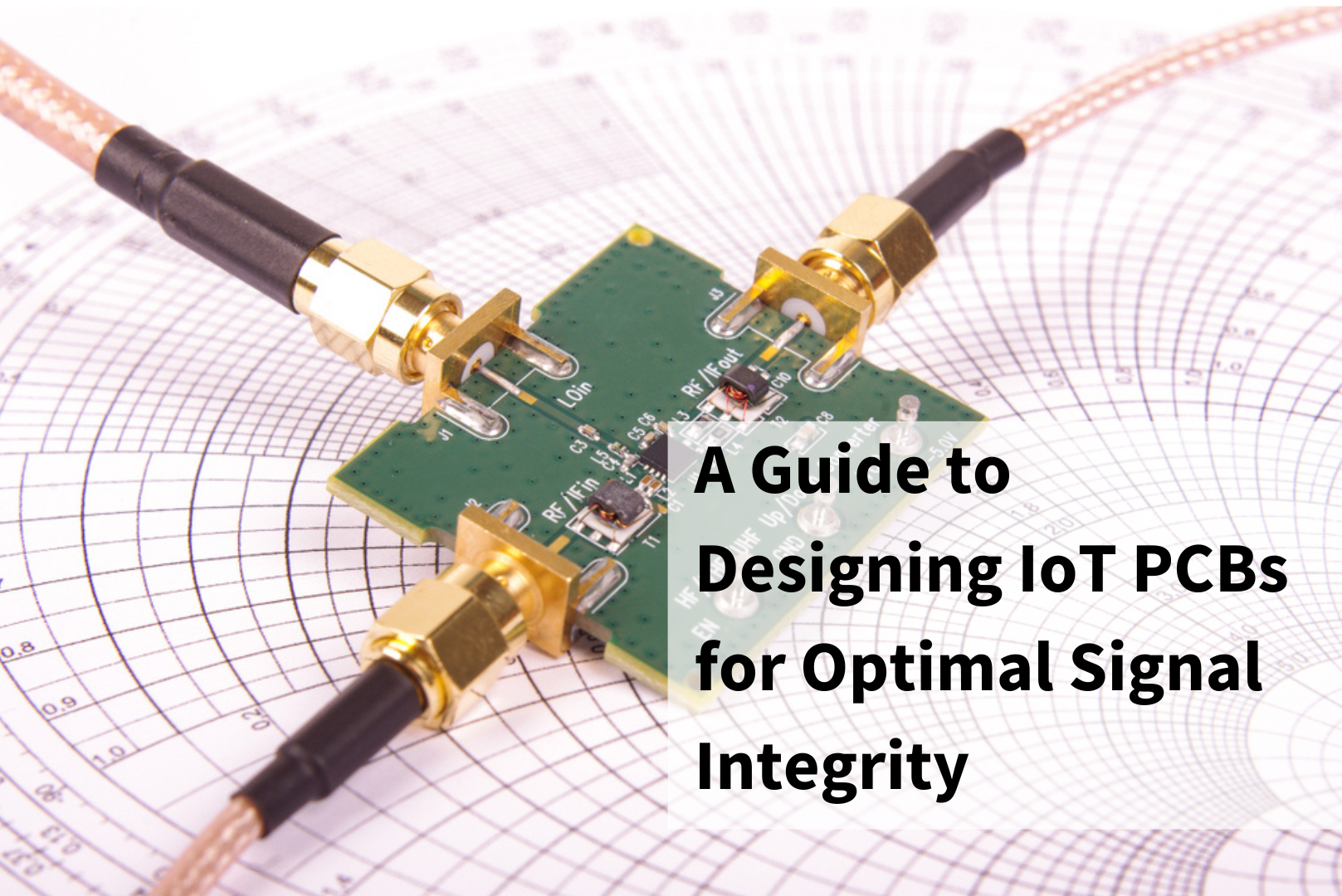
In this blog post, we'll look at why RF design and signal integrity are so important for IoT PCBs, how to achieve optimal signal integrity as well as the rules and factors you must keep in mind to ensure a smooth design and manufacturing process.
Table of Contents:
- The Importance of RF Design for IoT PCBs
- Starting the RF Design
- Dangers of Ignoring RF Rules
- Additional Rules and Regulation
The Importance of RF Design for IoT PCBs:
RF design on IoT PCBs is analogous to conducting a complex symphony. It dictates how wireless devices communicate, making it essential in an IoT environment. Neglecting RF issues might result in signal damage, poor range, and unreliable connections.
Achieving Optimal Signal Integrity Management:
-
Layout and Routing: Pay meticulous attention to trace routing. Maintain consistent trace widths, minimize bends, and avoid sharp corners to reduce signal reflections and interference.
-
Impedance Matching: Ensure that the characteristic impedance of transmission lines matches the impedance of the source and load. This prevents signal reflections and loss.
-
Ground Plane Design: A solid ground plane beneath the RF traces acts as a shield, minimizing interference and maintaining signal integrity.
-
Decoupling Capacitors: Place capacitors strategically to stabilize power supplies and minimize voltage ripples, which can affect signal integrity.
-
Isolation: Keep high-frequency components and traces isolated from sensitive areas to prevent cross-talk and interference.
Where to Start?

-
Easiest (and most straightforward): Maintaining consistent trace widths and using impedance calculators for proper trace width selection are relatively straightforward approaches.
-
Difficult: Advanced techniques like controlled impedance routing and extensive simulation using RF software demand a deeper understanding of RF principles.
Impedance matching is arguably the most crucial aspect of signal integrity management. It ensures that the signal is efficiently transferred from the source to the load, minimizing reflections and preserving signal integrity.
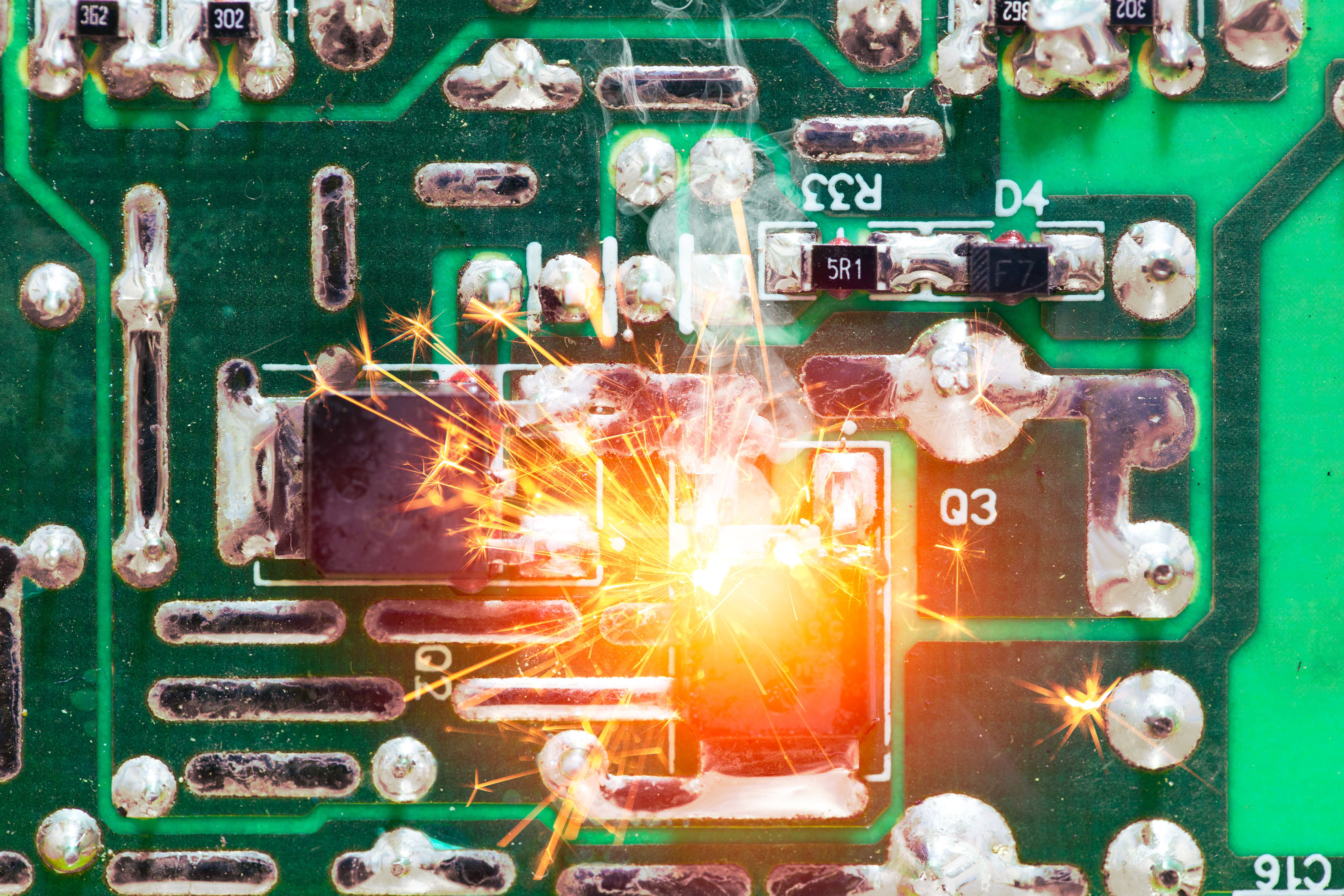
Dangers of Ignoring RF Design Rules:
Neglecting RF design principles can lead to numerous issues, including:
- Signal Degradation: Weakened signals result in reduced range and reliability.
- Interference and Cross-talk: Improper layout and isolation can lead to unwanted interference between traces.
- Limited Bandwidth: Inadequate RF design can restrict the bandwidth, affecting the device's ability to handle high-frequency signals.
Additional Rules and Considerations:
-
Antenna Placement: Ensure antennas are correctly positioned for optimal performance and minimum interference.
Read more about Antenna Optimization here: https://www.nexpcb.com/blog/integrating-antennas-into-pcbs-for-seamless-iot-connectivity
-
EMC Considerations: Address Electromagnetic Compatibility (EMC) issues early to prevent interference with other electronic devices.
-
Testing and Validation: Rigorous testing using RF equipment and simulation tools is crucial to verify the PCB's RF performance.
-
Manufacturability: Consider manufacturability constraints when making design choices, such as trace width and spacing.
-
Thermal Management: Heat dissipation is crucial for RF components. Adequate thermal vias and heatsinking strategies must be incorporated.

.png)


.png)