Wireless communication is at the heart of the revolutionary potential that these interconnected devices have in the fast-growing Internet of Things (IoT) world. The delicate dance of data exchange and communication between devices necessitates a strong foundation, and the Printed Circuit Board (PCB) is at the heart of that foundation.

1.PCBs designed for IoT applications require a specialized approach, carefully orchestrated to achieve seamless wireless connectivity while accommodating IoT devices' diverse functionalities.
The Convergence of Wireless Connectivity and IoT
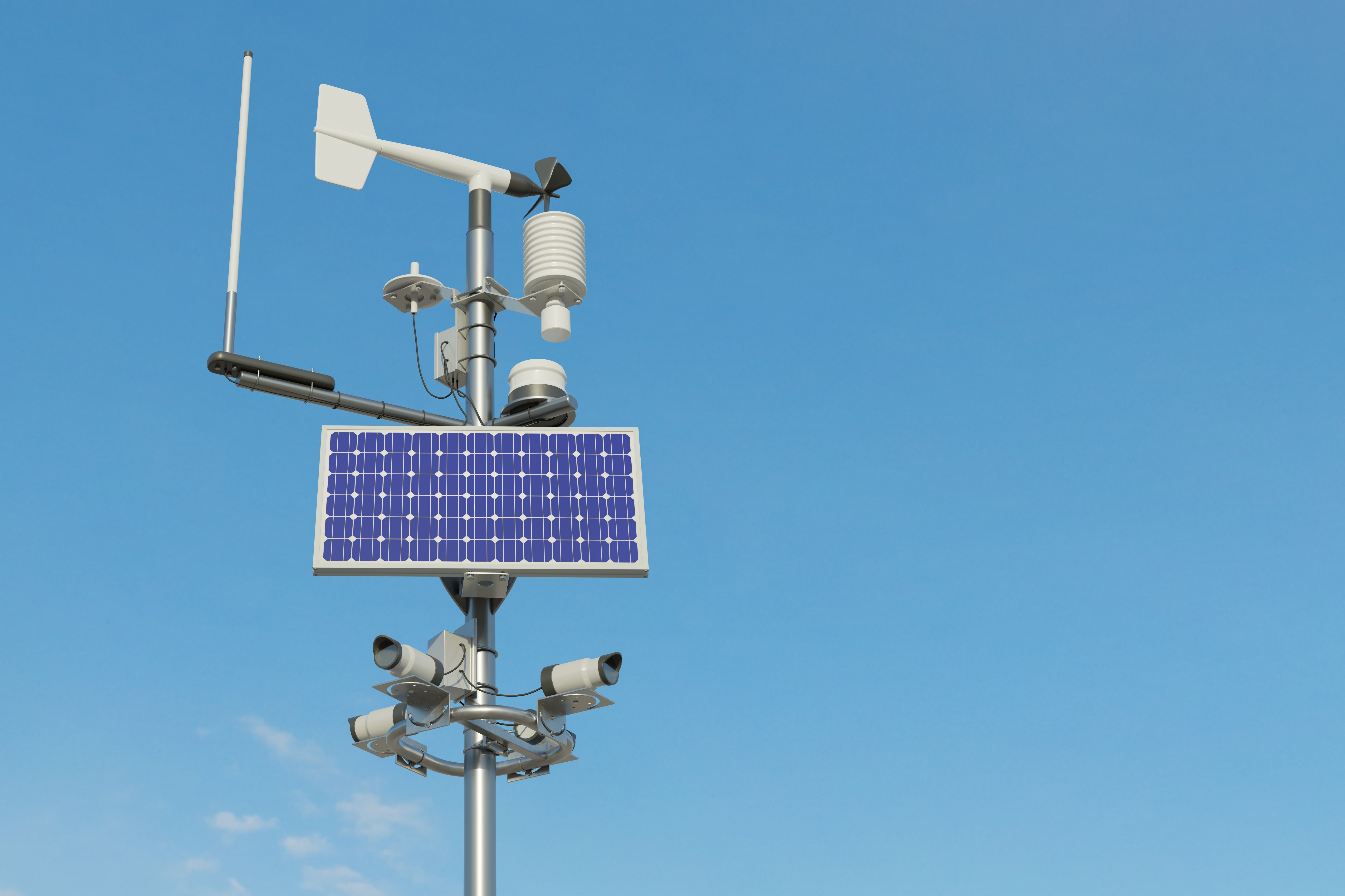
IoT devices are the conduits through which data flows, enabling objects, environments, and systems to communicate, analyze, and act on information. Wireless connectivity serves as the lifeline that binds these devices together, allowing them to share data, execute commands, and provide real-time insights. From smart homes and wearable devices to industrial automation and smart agriculture, IoT applications are only as powerful as the connections that underpin them.
PCBs, the intricate networks of conductive traces and components, play an integral role in enabling these connections. In the context of IoT, PCB design transcends the traditional boundaries of electrical engineering, embracing a multidisciplinary approach that includes radio frequency (RF) design, antenna integration, power management, and signal integrity considerations.
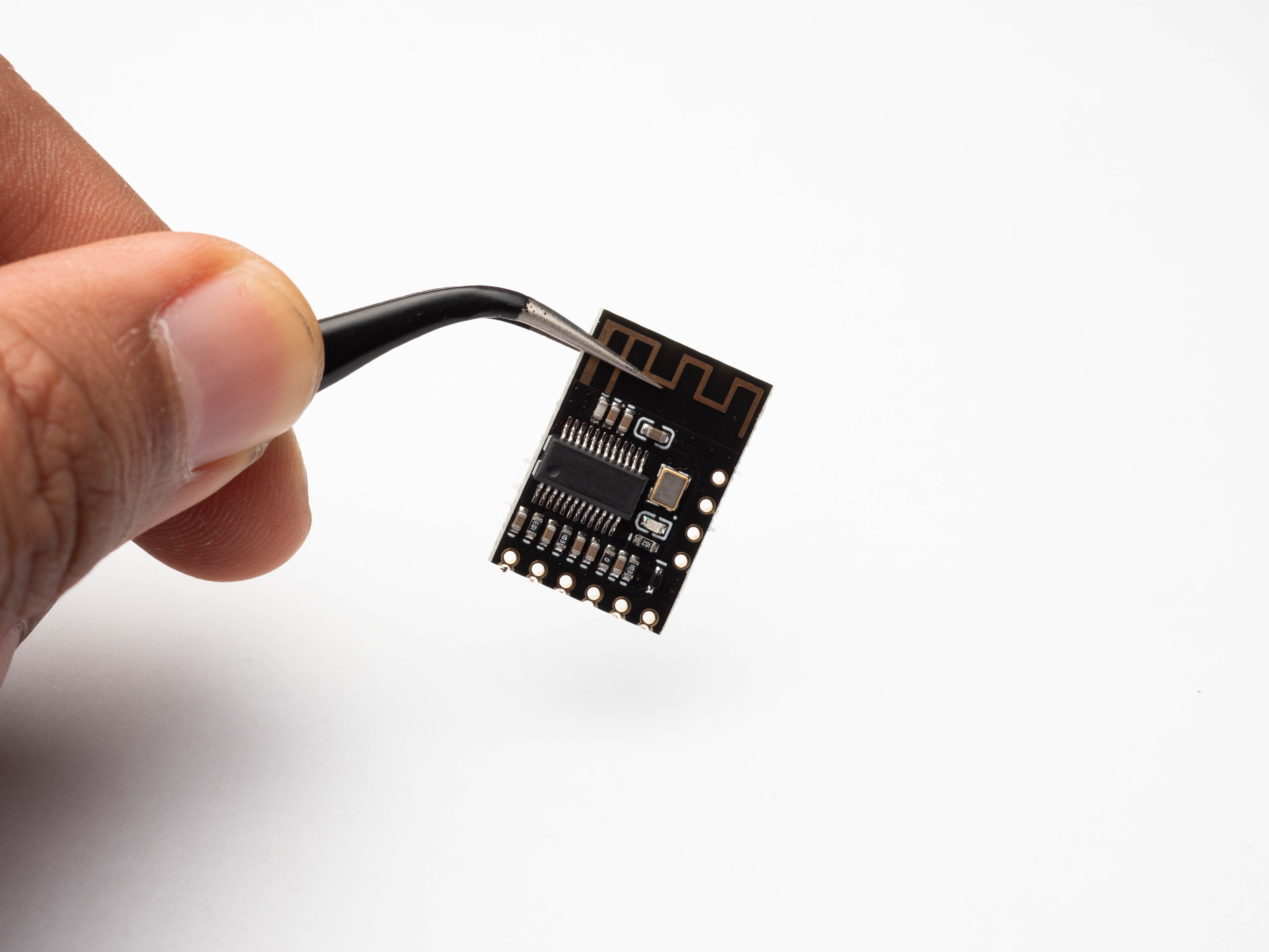
1. Antenna Integration and Placement
At the heart of wireless connectivity lies the antenna, the gateway through which devices communicate wirelessly. IoT PCBs must be designed with meticulous attention to antenna integration and placement. Antennas can be embedded within the PCB layers or positioned externally, depending on factors such as size constraints, frequency bands, and device form factor.
The dimensions and layout of the antenna trace are critical determinants of its performance. RF simulation tools and testing play a pivotal role in optimizing the antenna's impedance matching, radiation pattern, and gain. Moreover, the proximity of other components, such as metal shielding or ground planes, can impact the antenna's performance. Designers must strike a delicate balance between form and function to ensure the antenna's effectiveness.
2. RF and Signal Integrity
IoT devices often operate in crowded RF environments with multiple wireless protocols coexisting.
The 2 main purposes of PCB design to ensure smooth RF transmission and reliable wireless communication are:
1. Mitigate interference
Interferences, such as RF noise must be reduced to maintain clear communication paths. The strategies include:
- Ground plane design
- Component placement
- Careful routing
2. Ensure Robust Signal Integrity
Signal integrity or signal quality should always be maintained for proper communication. Signal integrity simulation tools aid in predicting and mitigating potential issues before physical implementation. Some techniques to ensure robust signal integrity includes:
- Controlled impedance traces
- Differential signaling
- Proper layer stack up
3. Power Management and Efficiency
Wireless IoT devices are frequently battery-powered, and power efficiency is a paramount concern. PCB design must consider power management strategies to extend battery life while ensuring uninterrupted connectivity. Low-power components, energy-efficient power supply designs, and intelligent power management circuitry are integral to achieving this balance.
Moreover, IoT devices may incorporate sleep modes to conserve power when not actively transmitting or receiving data. PCB design must facilitate seamless transitions between active and low-power states, ensuring that the device awakens promptly when needed while consuming minimal energy during periods of inactivity.
4. Multilayer PCBs and Miniaturization
IoT devices often demand compact sizes due to their diverse applications and form factors. Multilayer PCBs provide the necessary real estate for integrating various components, antennas, and routing while maintaining a small footprint. Miniaturization goes hand in hand with the IoT's mantra of "smaller, smarter, and connected."
However, the smaller the form factor, the more complex the design challenges become. Miniaturization requires careful consideration of trace widths, via placements, and component sizes. The designer's canvas is limited, necessitating a masterful symphony of efficient space utilization without compromising functionality.
5. Security and Connectivity
The importance of securing wireless communication on IoT devices cannot be emphasized enough. With the development of IoT devices, their vulnerability to cyberattacks increases. PCB design must incorporate security measures at various levels, including encryption, secure boot, and hardware-based authentication. Moreover, these security features must seamlessly coexist with wireless connectivity, ensuring that data remains protected while in transit.
Conclusion
Wireless connectivity is key for IoT, requiring PCB design to integrate seamless wireless connectivity with IoT functions. This fusion fuels a future where devices interact effortlessly, transforming how we interact with technology and the world.
.png)
.png)
.png)
.png)