In the rapidly expanding landscape of the Internet of Things (IoT), wireless connectivity stands as a cornerstone of the transformative potential these interconnected devices hold.
From smart homes and wearable devices to industrial automation and smart agriculture, the IoT ecosystem thrives on the ability of devices to communicate, analyze data, and provide real-time insights.
At the heart of this interconnected realm lies the delicate dance of data exchange, and the Printed Circuit Board (PCB) emerges as a pivotal canvas on which this dance takes shape.
Table of contents:
- Role of Antennas
- Why Integrate Antennas to PCBs?
- Challenges in PCB Antenna Integration
- Antenna Integration Approaches
- Design and Optimazion
The Role of Antennas in IoT Connectivity
Wireless connectivity is the lifeline that binds the diverse array of IoT devices together, allowing them to share data, execute commands, and interact with each other and the surrounding environment.
In this digital tapestry, antennas play the role of the conductor, orchestrating the symphony of communication.
Whether it's a wearable fitness tracker, a smart thermostat, or an industrial sensor,
antennas are the conduits that translate data into electromagnetic signals, transmitting and receiving information across the airwaves.
Why Integrate Antennas into PCBs?
The integration of antennas directly into PCBs offers several compelling advantages for IoT devices:
- Space Efficiency: IoT devices often demand compact sizes due to various form factors and applications. By embedding antennas within the PCB layers, the available space is maximized, allowing designers to create sleek and streamlined devices without sacrificing connectivity.
- Enhanced Aesthetics: Antennas integrated into PCBs contribute to a cleaner and more aesthetically pleasing device design. External protruding antennas can be eliminated, resulting in a more polished appearance that aligns with the desired product aesthetics.
- Improved Durability: External antennas are vulnerable to physical damage and environmental factors. Embedded antennas are shielded within the device, offering improved protection against wear and tear.
- Radio Frequency (RF) Performance: PCBs with integrated antennas can be optimized for better RF performance through careful layout and design. This ensures efficient signal transmission, and reception, and reduced signal interference.
- Cost Efficiency: By utilizing the PCB itself as part of the antenna structure, manufacturing costs can be reduced by eliminating the need for additional components and assembly steps.
Challenges and Considerations in Antenna Integration
The integration of antennas into PCBs for IoT devices presents a set of challenges and considerations that must be carefully navigated to ensure optimal performance:
1. Frequency Bands and Resonance:
IoT devices often operate across different frequency bands, depending on the wireless protocol (e.g., Wi-Fi, Bluetooth, Zigbee, LoRa). Antenna designs must be tailored to resonate at the specific frequency of interest to achieve efficient communication.
2. Form Factor and Size Constraints:
The dimensions of the PCB and the device's form factor significantly impact the antenna design. Smaller devices necessitate compact antenna designs that maintain suitable radiation patterns and gain.
3. Antenna Efficiency and Gain:
Antenna efficiency is crucial for effective communication. Efficient antennas ensure that most transmitted power is radiated as electromagnetic waves rather than being lost as heat. Gain, which represents the antenna's ability to focus radiation in a specific direction, is another vital parameter.
4. Matching Network Design:
To maximize signal transmission and reception, antennas must be impedance-matched to the RF circuitry. Designing proper matching networks ensures that the antenna's impedance matches that of the connected components, preventing signal reflections and losses.
5. EMI and RF Interference:
Proximity to other PCB components, traces, and layers can impact the antenna's performance by introducing electromagnetic interference (EMI). Careful layout and shielding techniques are essential to minimize EMI effects.
6. Simulation and Testing:
Antenna integration requires extensive simulation and testing to optimize performance. Tools like RF simulation software help predict radiation patterns, impedance, and other critical parameters before physical implementation.
Approaches to Antenna Integration
Several approaches are used to integrate antennas into PCBs, each tailored to the specific needs of the IoT device:
1. Planar Inverted-F Antenna (PIFA):
The PIFA is a popular choice for IoT devices due to its compact size and versatility. It consists of a metal trace on the PCB's top layer, often designed in the shape of an inverted "L" or "F." PIFAs can be tuned to resonate at different frequencies by adjusting their dimensions.
 source: Digikey
2. Printed Monopole Antenna:
This type of antenna is created by printing a monopole structure on the PCB's surface. It is simple to manufacture and offers a wide bandwidth. Printed monopoles are commonly used in applications where size constraints are less stringent.
source: IEEE Explore
3. Slot Antenna:
Slot antennas are etched into the PCB's ground plane, typically in the form of a narrow slot or rectangular cutout. They offer good radiation patterns and gain, making them suitable for applications requiring higher performance.
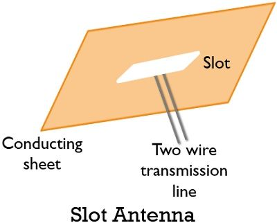
source: Electronic Desk
4. Microstrip Patch Antenna:
Microstrip patch antennas consist of a patch of conductive material on the top layer of the PCB, backed by a ground plane on the bottom layer. They are compact and versatile, offering directional radiation patterns.
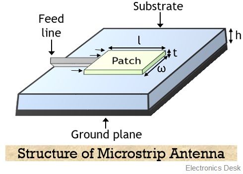
source: Electronic Desk
Design and Optimization
The design of antennas for IoT PCBs involves a multi-faceted optimization process to achieve the desired performance characteristics:
- Simulation Tools: RF simulation software plays a pivotal role in predicting the antenna's radiation pattern, impedance, and gain. It allows designers to iterate through different design options and make informed decisions.
- Matching Network: Designing matching networks that ensure impedance matching between the antenna and RF circuitry is crucial. These networks optimize power transfer and minimize signal loss.
- Materials and Substrates: The choice of PCB materials and substrates impacts the antenna's performance. High-quality materials with suitable dielectric constants are chosen to ensure proper impedance matching and radiation efficiency.
- Physical Layout: The physical layout of the antenna on the PCB must consider factors such as ground plane proximity, component placement, and isolation to minimize interference and enhance performance.
The integration of antennas into PCBs for IoT applications marks a pivotal step in realizing the seamless wireless connectivity that defines the IoT landscape. As devices become increasingly interconnected and the demand for efficient, reliable communication grows, antennas embedded within PCBs play a vital role in bridging the physical and digital worlds.
.png)


.png)