In PCBs, the ground could take different forms; ground planes, which were indicated by patches or a whole layer of copper, or simply just an external jumper that could be connected to the negative port of an external supply source.
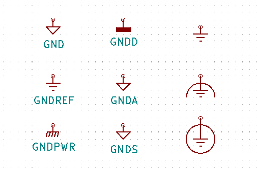
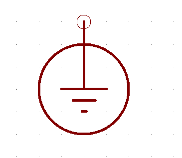
In general applications, the GND or ground symbol was to be indicated by the following symbol. The symbol could often be seen in circuit schematics: logical, electrical, etc.

1. Power ground
Power ground, or chassis ground, which could simply be understood as the negative end of the power supply, or the metal casing of your designed system.
The power ground is commonly used if any potential difference between the metal case (or power supply’s ground) and the real ground is present.

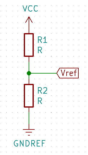
Reference Ground refers to the ground used for the return stage after referencing a voltage source as an input, i.e. Vref. An example of the use could be seen below using a potential divider circuit.
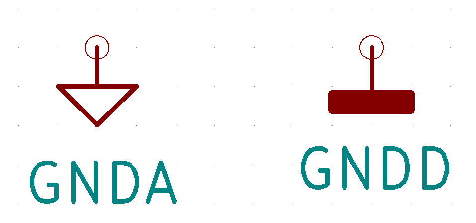
2. Signal Ground
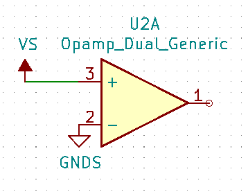
Signal ground indicates the ground which is used for a reference voltage. Implementing it as a comparator input, for example, would be useful to control the shape of the said input signal.
Besides the generic signal symbol shown in the picture above, specific signal GND symbols (i.e., digital and analog) could also be used to provide a better description of the system.
3. Protection Ground (Earth)


 On the other hand, the protective earth ground indicates that the connection should be very well insulated to prevent any unwanted contacts from the board’s users. This was usually applied in the form of fuses and circuit breakers, which disconnect the circuit at times where the circuit’s current or voltage gets too high, which could potentially cause burning or even worse, explosion in the system.
The discussion led us to one important question, “Are this all necessary for PCB construction?" The answer is no. If there were no special conditions that need to be taken into account, it’s all right to use the general ground symbol of GND for construction, allowing easier and cheaper production of the PCB.
Are ground planes always needed for PCB construction? Again, no. Usually, in power electronics applications, the inputs and outputs of the system are very often isolated, hence adding the ground plane layer would break the isolation. However, when constructing more complex PCBs with more than 2 layers, adding the ground plane would be very much useful since isolation could still be maintained.
.png)
.png)
.png)
.png)