1. Line Width/Space and Security Requirements
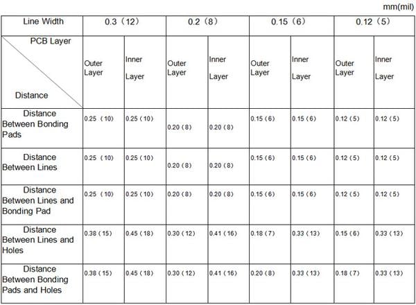
When the packing density is permissible, choosing a lower-density routing design to improve reliability and defect-free manufacturing capacity. Current manufacturers’ processing capacity is: minimum line width/spacing is 3mil/3mil. Common routing density designs refer to the following table.
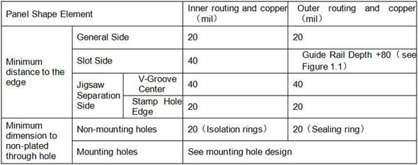
The distance from inner and outer routing to the panel edge, the distance from the copper to the panel edge, and the dimension of non-plated through hole must be satisfy the requirements in the table below.
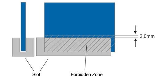
1.1 Guide Rail Depth
There must be no routing in the area where devices with metal shell (such as radiators, power modules, horizontal voltage regulators, and ferrite inductor, and etc.) directly contact with the PCB, in addition, extending outward 1.5mm of this area is the forbidden zone for surface routing. Shown in Figure 1.2.
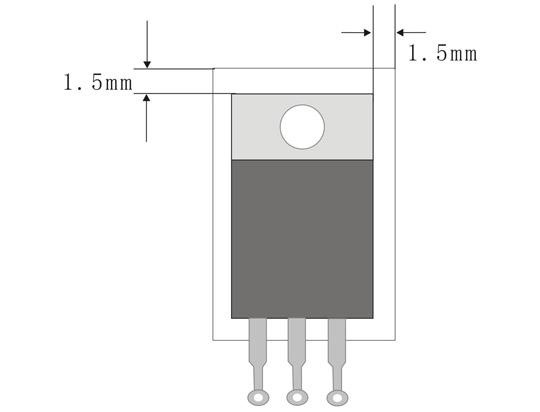
1.2 Forbidden Zone for Surface Routing of Devices with Metal Shel
2. Routing Ways
When circuit is connected with devices, in principle they can connect at any point. However, for reflow soldering devices, the design should follow the principles below:
Devices like resistance and capacitor jointing on two bonding pads should be connected with the printed routings that go outlet equally to the line width from the central position of the bonding pad. Outgoing lines whose width is smaller or equal to 12 mil don’t have to follow the rule. Line width must not exceed the minimum side length of bonding pad.
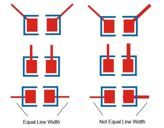
2.1 Requirements for Line Width
a) Devices must go outlet from the central head face of the bonding pad.
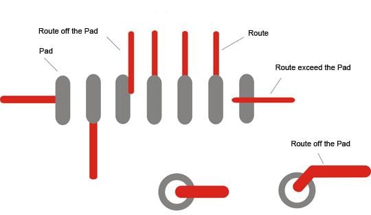
2.2 Outlet from the Central Bonding Pad
b) When the routing connecting with bonding pad is wider than bonding pad, it cannot cover the bonding pad that it should route from the end of bonding pad; when fine-pitch SMT bonding pad pin needs to be connected, it should be joint from the outer of the pin rather than the middle.
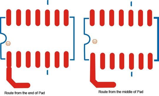
2.3 Requirement 1 for Bonding Pad Routing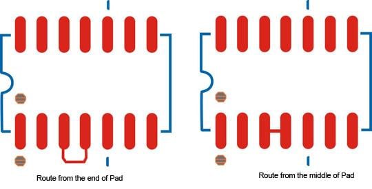
2.4 Requirement 2 for Bonding Pad Routing
c) The routing going through BGA holes and connecting with the bonding pad needs to use the way of dog bones. See in 2.5.

2.5 Joint through BGA Holes to Bonding Pad
3. Copper Polygon
If there is a large area without linear and graphics of the outside, it is recommended to be covered by copper grids in this zone to make the whole panel surface of copper spread evenly. The size of square in the copper grids is about 25mil x25mil.
Note: The inside layer doesn’t need copper grids design.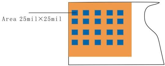
3.1 Large Area Copper Grid Design
When large area of devices from the power zone and ground terminal zone connect with bonding pads, they should be designed into the shape shown in the following graph, so as to avoid large area of copper heat too fast to affect soldering quality or cause a cold solder joint.

3.2 Large Area Copper and Joint of Devices and Bonding Pads Design
If you want to learn more about PCBA, we highly recommend you to check the following articles:
Posted by Candy Xu

Candy has helped numerous startups and makers get their hardware across turbulent seas of the market into their customers' hands. Having studied engineering, she's all round equipped to solve problems in all aspects of our services.
