In PCB (Printed Circuit Board) design, it is best not to exceed the batch-production technology level of manufacturers. Otherwise, the PCBs may not be able to be processed, or have high associated costs.
1.1 Range of Dimensions
The ideal dimensions for production are as follows: width (200mm-250mm), length (250mm-350mm). For a PCB with length shorter than 125mm or width shorter than 100mm the panelization method can be used to transform the dimensions of the PCB to ideal values according to requirements of production. This facilitates component insertion and soldering.
1.2 Shape
a) The shape of the PCB is rectangular. If a PCB does not need a panel, the four corners of the plate must be rounded as shown in Figure 1.2.1. If a panel is needed, the four corners of the PCB must be rounded after being panelized, with radius 1mm-2mm.
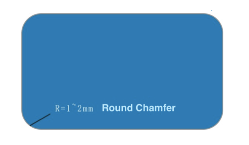
Figure 1.2.1 Schematic Diagram of PCB Shape
To ensure stability in the transmission process, the penalization method is used to transform irregularly shaped PCBs. Specifically, the gap on the corner must be supplemented, as shown in Figure 1.2.2. Otherwise, special tooling design is needed.

Figure 1.2.2 Schematic Diagram of Technological Panelization
b) To ensure that the PCB is stably transferred by chains, any gap on a pure SMT must have length shorter than 1/3 of the corresponding edge, as show in Figure 1.2.3.
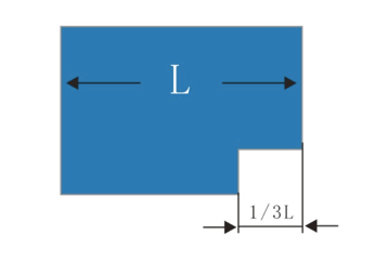
Figure 1.2.3 Permitted Size of Gap
c) Figure 1.2.4 shows design requirements for gold fingers: chamfers are designed on the insertion edge as required; (1-1.5) x 45o chamfers or (R1-R1.5) circular beads should be designed on the two sides of the insertion board to facilitate insertion.

Figure 1.2.4 Design of Chamfer of Gold Fingers
1.3 Technology Edge
For a PCB without a technology edge, scopes that are 5mm or further than 5mm from the positive or negative edges of the board cannot have any components or soldering spots; and the wiring position must be at least 3mm from edges of the board. If short-insertion wave soldering is adopted, the board must meet the width requirements of general transfer edges, and the height of components 10 mm from board edges must be limited to 40 mm (containing the thickness of the board), in consideration of the characteristics of short-insertion wave braziers, as shown in Figure 1.3.1.

Figure 1.3.1 Schematic Diagram of PCB Transfer Edge
If the size of the keep-out area on the transfer edge of the PCB board cannot meet above-stated requirements, a 5mm or wider processed edge must be added to the corresponding board edge. The smoothing radius of the processed edge is 2mm, as shown in Figure 1.3.2.
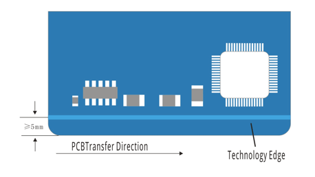
Figure 1.3.2 Design Requirement 1 of PCB Technology Edge
To meet the special requirements of structural design, if a component protrudes from the transfer edge of the PCB, the width of the auxiliary edge must meet the requirements shown in Figure 1.3.3.
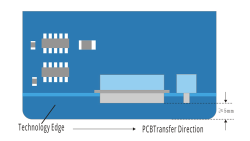
Figure 1.3.3 Design Requirement 2 of PCB Technology Edge
1.4 Fiducial Mark
Fiducial marks are needed for the placement of equipment adopting optical locations. They are used for overall automatic location of chip mounters, and must have high contrast ratios when illuminated by a chip mounter.
1.4.1 Design of Fiducial Marks
Requirements of appearance design of fiducial marks are as follows:
1. Solid circle;
2. Inner diameter = 1mm;
3. Ring-shaped radius of the solder mask is 0.5mm, as shown in Figure 1.4.1.
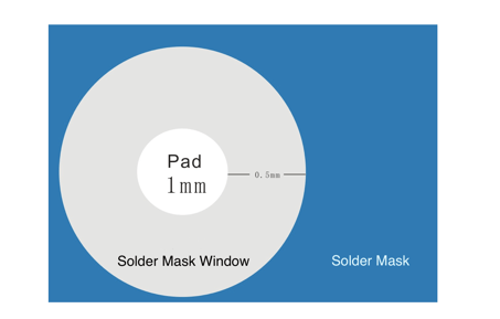
Figure 1.4.1 Schematic Diagram of Fiducial Mark
1.4.2 Application of Fiducial Marks
Fiducial marks are mainly applied to panel, plate and local positions, as shown in Figure 1.4.2.
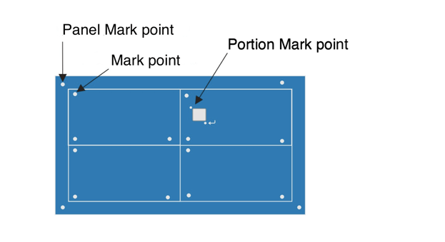
Figure 1.4.2 Application of Fiducial Marks
1.4.2.1 Global Fiducials
Three fiducials must be selected from the four corners of the board. If both the surfaces of the board have placement components, each surface must have fiducial mark, as shown in Figure 1.4.3.

Figure 1.4.3 Location of Fiducial Mark on the Plate
1.4.2.2 Panel Fiducials
Global fiducial marks of three panels are required. The diagonal point of each panel should have at least two fiducial marks. In special situations, you must negotiate with technologists to determine whether the two fiducial marks on two panels can be omitted or not. However, the global fiducial marks of the panels must be reserved.
1.4.2.3 Local Fiducials
The lead pin pitch is smaller than 0.4mm. For QFP packaging chips with more than 144 lead pins, two marks at opposite corners of the chip need to be increased. If the above-stated components are close (with distances smaller than 100mm), they can be regarded as a whole, and two local fiducials need to be increased on the diagonal position, as shown in Figure 1.4.4.
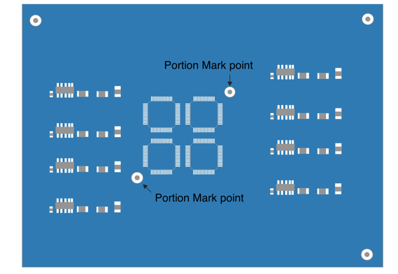
Figure 1.4.4 Local Position of Fiducial Marks
If you want to learn more about PCB design, we highly recommend you to check the following articles:
Posted by Candy Xu

Candy has helped numerous startups and makers get their hardware across turbulent seas of the market into their customers' hands. Having studied engineering, she's all round equipped to solve problems in all aspects of our services.
