There are two problems to consider when design panel: one is how to place the boards; and the other is the way of connection.
1. Panel Layout
Panel can increase productivity and save on production costs; the first thing to consider in panel design is how to place small plates together to make a lager board. It is recommended that the basis of panel design is when the final size is close to the ideal size.
1.1 PCB board’s long side length ≥ 125mmWhen PCB board’s long side length ≥ 125mm, the boards can be placed as Figure 1.1 shows. The perfect number of boards is achieved when the final size is consistent with as (Figure1.2.1) requires. The stiffness of this placement is beneficial for the wave-soldering. Figure 1.1(a) is a typical panel, and Figure 1.1(b) is suitable for the situation that the rounded corners required after the separation of daughter boards.
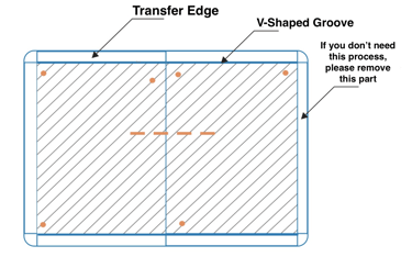
(a) V-shaped groove separating method
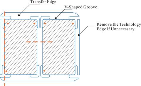
(b) Slotted hole separating method
Figure 1.1: Panel
When PCB board’s long side length < 125mm, the boards can be placed as Figure 1.2 shows. The perfect number of boards is achieved when the final board length is consistent with as Figure1.2.1 requires. When this method is used, the rigidity of boards should be concerned. Figure 1.2 (a) is a typical V - shaped groove separated panel, there are three perpendicular craft edges to the PCB transfer direction with double-sided deposited copper foil, to enhance the stiffness. Figure 1.2 (b) is suitable for the situation that the rounded corners required after the separation of daughter boards, and the joint stiffness of separated sides paralleled to the PCB transfer direction should be concerned.
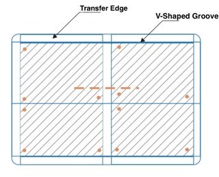
(a)V-shaped groove separating method
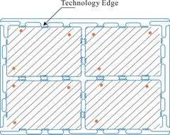
(b) The Long Slot plus a Small Circular Hole Separating Method
Figure 1.2: Panel
1.3 Panel of Sketch PlatePay attention to the connection between panel and panel, and try to keep each separated connection in a line, as 1.3 shows.
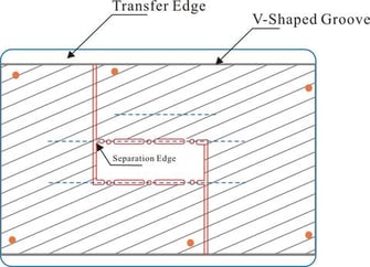
(a) L Shaped Panel
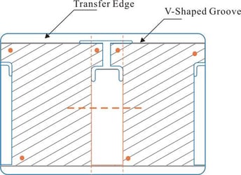
(b) T Shaped Panel
Figure 1.3: Panel of Sketch Plate
2. Connection of Panel
There are two main connection methods for panel: Double face carved V-shaped groove (V-CUT), and the long slot plus a small circular hole (commonly known as stamp hole), depending on the shape of the PCB.
2.1 V-CUT connection methodWhen it is straight-lined connection between plate and plate, the plate margin is neat and does not affect devices installation; the V-CUT method can be used. V-CUT is a through type, and cannot turn in the middle. Currently SMT Board is widely used, characterized with neat and level edges after separation and low processing costs, which is recommended as priority.
a) The two sides of V-CUT line (A side and B side) require a no device and no wire area that is not smaller than 1mm, to avoid the damage to devices and wires when separating.
b) After cutting the V-shaped groove, the remaining thickness X should be 1/4 to 1/3 of the board thickness Y, which is not smaller than 0.4mm. Board bears heavier can take upper limit, and vice versa. The misalignment of the upper and lower sides cut S of V-shaped groove must be less than 0.1mm.
The design requires being consistent with Figure 2.1.
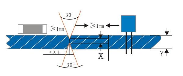
Figure 2.1 Design Requirements of V-Cut
2.2 The Long Slot plus a Small Circular Hole Connection MethodThe connection method of long slot plus a small circular hole, also known as stamp hole method, is suitable for any shapes of daughter boards. As the margin area is not neat and level after separation, it is not recommended for those PCB with fixed conduit ferrule.
Requirements for the long slot plus a small circular hole method: The width of long slot is usually between 1.6mm and 3.0mm, and the length is about 25mm to 80mm, the connection bridge between slot and slot is generally 5mm to 7mm, with several small circular holes placed, and the diameter Ф of these holes is 0.8mm ~1 mm, the distance from the center of the aperture to the outside is 0.4mm – 0.5mm: Thicker boards take smaller value and thinner boards take larger value, it is a typical value in Figure 2.2. The length of the cutting groove is based on the PCB routing directions, assembly process, and the size of PCB. The smaller the aperture, the neater the margin area.
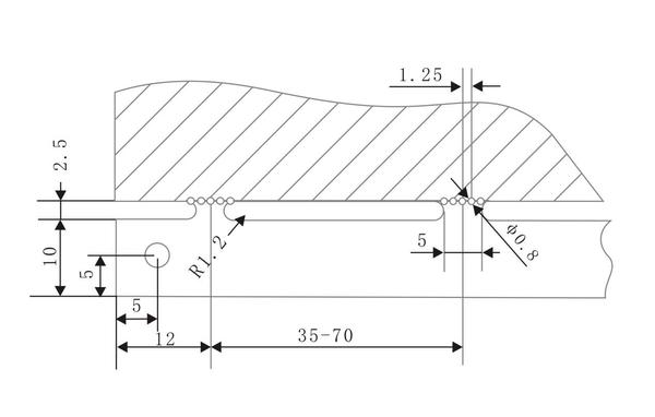
Figure 2.2 The Long Slot plus a Small Circular Hole Method
2.3 The Design of Connection BridgeWhen design connection bridge, it is mainly to consider: whether the margin area after separation is neat or not; whether it is convenient to separate or not; is the stiffness enough for production; the material, thickness and total weight of single plate; the distance between connection bridges (the recommended distance is 60mm). In order to make the margin area neat after separation, the separating holes are usually placed on the sidelines or slightly within the daughter board.
If you want to learn more about PCB design, we highly recommend you to check the following articles:
Posted by Candy Xu

Candy has helped numerous startups and makers get their hardware across turbulent seas of the market into their customers' hands. Having studied engineering, she's all round equipped to solve problems in all aspects of our services.
