1. General Rules for Components Placement
a) THD components with polarity or direction are required to place in the same direction, and as neat as possible. For SMD components that cannot meet the requirement of staying in the same direction, just try to keep them in the same X or Y direction, such as Tantalum capacitor.
b) To pay attention to the location of radiator for SMD, and to leave enough space to make sure that the radiator will not touch other components, the minimum distance requirement is 0.5mm.
c) Thermosensors (such as electrolytic capacitors, crystal oscillators, and etc.) should be kept far away from high heat elements; and they should be placed on the windward side; and high components should be placed behind low components along with the direction of the least wind resistance, so as to prevent air duct from being blocked.

1.1 The placement of thermosensors
d) No touching or stacking of components to meet the space requirements of component installation.
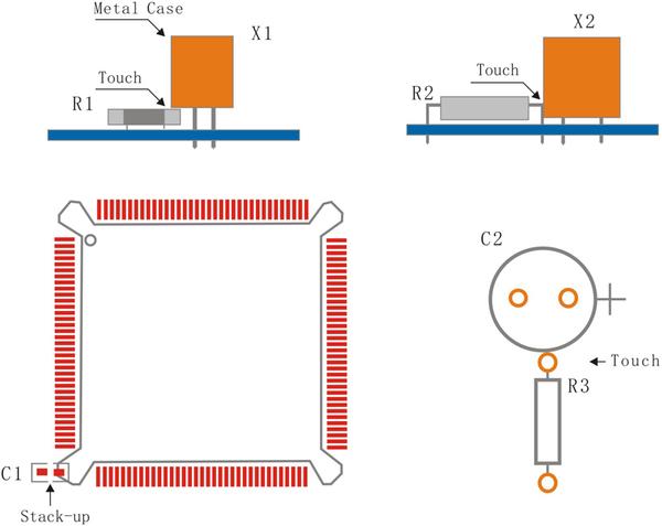
1.2 Bad Placement examples
e) High-heat-load components, such as power inductors or power regulators, cannot be placed to get too close to the technology edge (or panel edge), and the distance to the edge must be above 20mm, which is in order to avoid temperature goes uneven of reflow oven guide rail that may affect soldering.
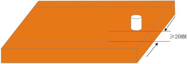
1.3 The distance between high-heat-load components and technology edge (or panel edge)
f) High-heat-load components, such as power inductors or power regulators, cannot be placed closely to each other. This includes the positive and negative sides, and the distance between each other must be 20mm or above, which is to avoid large PCB partial heat load.
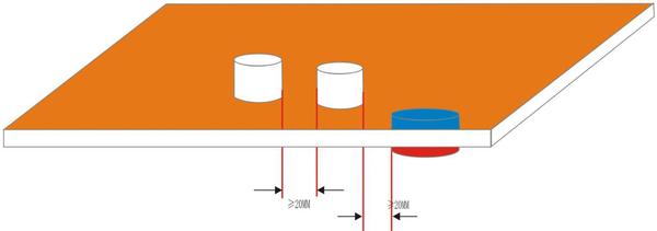
1.4 The distance between high-heat-load components
2. Requirements for THD Component Placement
a) Except for structural components with special requirements, all the THD components must be placed on the positive side.
b) The distance between adjacent components is shown in figure 2.1.

2.1 The distance between adjacent components
c) To meet the operating space of manual soldering, maintenance and inspection requirements, as shown in Figure 2.2.
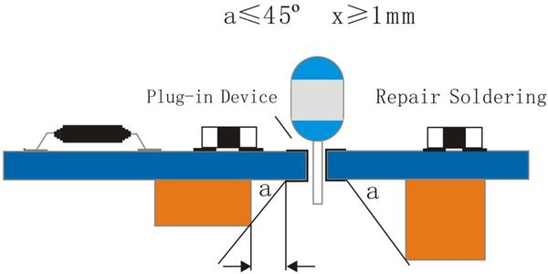
2.2 Searing-iron operating space
d) When components are placed on one side of plug-in components, the minimum bonding pad edge space can be processed for parallel soldering joints placement is 3.0mm; if it is the vertical soldering joints placement, the minimum bonding pad edge space that can be processed is 1.0mm; see figure 2.3.
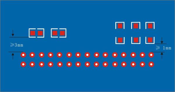
2.3 One side SMD components placement
3. SMD Components Placement Requirements
a) Fine-pitch components (including BGA, 0.4mm, and 0.5mm QFP) are recommended to be placed on the same side.
b) Polar patches are arranged in the same direction as much as possible, and the visual angle required will be less than 60o; as the soldering joints inspection will be affected if higher components are placed close to lower components; as shown in 3.1.
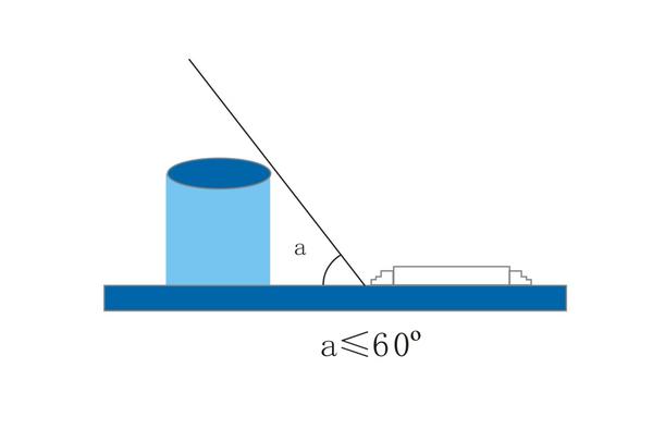
3.1 Soldering joint points visual inspection
c) There must be forbidden zone around the BGA components( BGA).

3.2 Requirements of the forbidden zone between BGA and othercomponents
d) 2mm forbidden zone must be left out around QFN.
e) 2mm forbidden zone must be left out around module.
f) It is not recommended that two SMD wing shaped pin to overlap as a compatible design. Take SOP packages as an example, shown in figure 3.3.
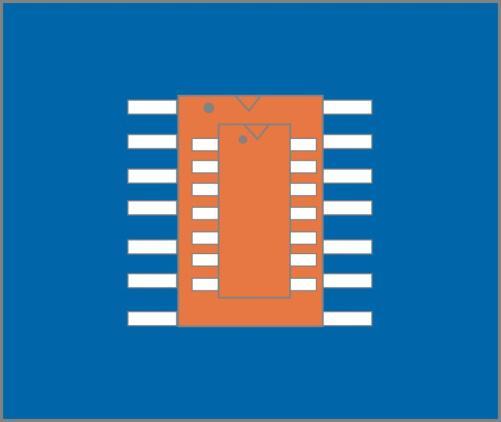
3.3 Two SOP packages components compatible design
g) It is allowed to design THD and SMD stacked together when there is no influence on the THD soldering by the SMD bonding pad and the solder paste printed on it. The following figure 3.4 shows the example of DIP-8 and SOIC-8 packages components compatible design.
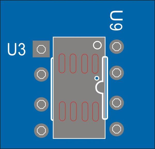
3.4 DIP-8 and SOIC-8 packages components compatible design
h) Requirements for the distance between SMD: same kind of component: ≥0.5mm; different kinds of component: the distance should meet the requirements of soldering joints inspection, which requires the visual angle ≤60o.
Note 1: The measurement volume of distance value is chosen the larger one from the ponding pad and componentitself.
Note 2: When the lower SMD ponding pad is placed closely to the higher component, the distance between them should meet the requirement of soldering joints inspection, which means the visual angle should be less than 60 o. See figure 3.5.
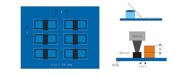
3.5 Distance requirement of components placement
i) The distance between fine-pitch components and the panel routing edge should be more than 10mm; otherwise, it will affect the solder paste print quality.
j) The distance between other non-fine-pitch components and the panel routing edge should be more than 5mm, and the distance between other non-fine-pitch components and the non-transmission side panel edge should be more than 3mm. see figure 3.6.
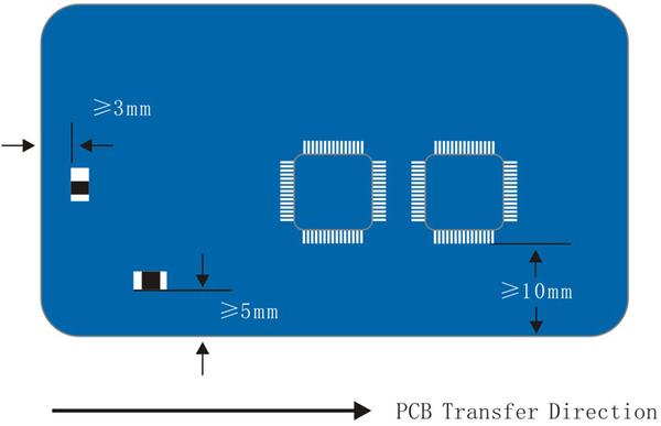
3.6 Requirement of forbidden zone between SMD and panel edge
If you want to learn more about PCBA, we highly recommend you to check the following articles:
Posted by Candy Xu

Candy has helped numerous startups and makers get their hardware across turbulent seas of the market into their customers' hands. Having studied engineering, she's all round equipped to solve problems in all aspects of our services.
