With the development of the e-commerce and logistics industry, we could easily finish a product design in America and send it to the Chinese team by 8: 00 PM EST, which allows the Chinese team to receive this product design by 8:00 AM local time. If artwork can be immediately and fully confirmed, the stencil can be produced within one day and sent back to America the following afternoon by UPS.
How to generate a PCB stencil file
Communication during production is extremely important. It is necessary in order to create the most accurate and professional stencil files. While designing certain samples, it is necessary for the stencil file to be able to be opened by the following software:
How to export a PCB stencil file
Knowing how to export a PCB stencil file from different design software accurately is vitally important. The available methods for exporting a stencil file from different PCB design software are:
1.PCB design software:
2.Other professional CAD/CAM software:
Let’s take for example converting to Gerber in Protel99SE
Step 1: Click  Protel Stringon the tool column, use the mouse to double click. The software will pop-up below the dialogue box.
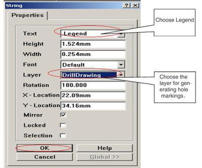
Step 2: Press OK and then select the suitable place for this string.
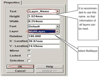
Step 3: Begin converting the Gerber file. Press CAM Manger to start the Output Wizard for exporting Gerber files.
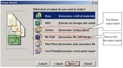
Select the “Gerber (Generates Gerber files)” option and press NEXT to continue.
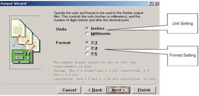
As indicated above, press NEXT to continue with all default values.
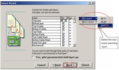
Select the expected exporting layers and press NEXT.
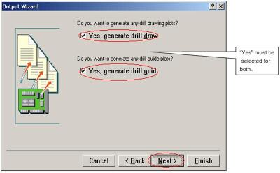
Press NEXT and the window below will appear.
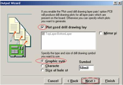
Press NEXT.
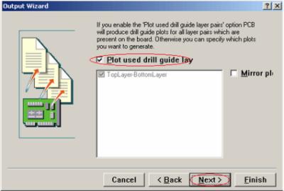
Press NEXT.
Press FINISH to complete. Now the file has been successfully converted to Gerber. Do not export Gerber files yet.
Step 4: Press Tool——Scan Wizard, the system will pop-up below the dialogue box.
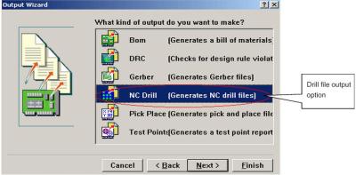
Select NC Drill to convert to NC Drill.
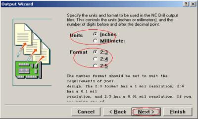
Press NEXT.
Press FINISH to complete converting. Now the drilling level has been successfully converted.
Step 5: Press Tools – Preferences as pictured below.
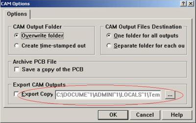
It is unnecessary to select a specific destination folder as the PCB drawing library is default, allowing later exportation from that location.
Step 6: Select the required Gerber file export folder and press OK. Select the following options:

Press F9 to export the Gerber file. Gerber has now been successfully converted and stored in the appointed folder. Next, use CAM software for processing.
PCB stencil file check list
Before sending a PCB SMT stencil file to the factory, it is necessary to check it over thoroughly. Especially pay attention to the following areas:
- Checks to see if there are any errors in the sequence or position of the plate in the stencil.
- Checks the PCB drawing size, makes sure the SMT stencil fits the PCB well.
- Checks the material requirements of the PCB SMT stencil.
- Checks the thickness requirements of the PCB SMT stencil, normally the thickness is 0.13mm or 0.1mm.
- Checks to see if all the drilling data is correct.
PCB stencil manufacturing technologies
The two main PCB SMT stencil manufacturing technologies used are PCB chemical etching and PCB laser cutting. The quality of the aperture walls is how PCB SMT stencil are valued these days, with rougher edges characterizing an inferior PCB SMT stencil. The progressing of laser technologies has led to this manufacturing process becoming much more mainstream.
PCB chemical etching:
Uses the processed Gerber data to guide a photo-plotter in producing a film, transfers the film to a steel plate and uses an etching machine for processing.
PCB laser cutting:
Imports the processed Gerber data into the laser machine and uses the computer to control the laser machine to drill holes onto the SMT stencil.
You can see how it works out from the following video.
http://www.youtube.com/watch?v=Toaz0Hi3miY
If you want to learn more about PCB design, we highly recommend you to check the following articles:
Posted by Candy Xu

Candy has helped numerous startups and makers get their hardware across turbulent seas of the market into their customers' hands. Having studied engineering, she's all round equipped to solve problems in all aspects of our services.


