1.Design of bonding pad with through hole cartridge components
a) The diameter design of components plug-in holes is according to the leading wire diameter, the lead shaped condition, and wave soldering process. In consideration of soldering process, it is better to choose standard size of hole’s diameter. In addition, on the same circuit panel, the standards of holes’ diameters should be as less as possible. In order to reduce the process cost, irregularly shaped holes should be avoided.
b) The difference between the diameter of cartridge components lead (cylinder-shaped) and the diameter D of plug-in hole should be from 0.40mm(16mil) to 0.60mm(24mil),that is the gap L between the plug-in hole and the device component leading wire should be ranged from 0.20mm(8mil) to 0.30mm(12mil) so that it is easier to plug in and increase the reliability of soldering.
c) The difference between the diagonal length of cartridge components lead (rectangular) section and the diameter of plug-in hole should be 0.20mm(8mil)~0.25mm(10mil), that is the gap between the plug-in hole wall and four corners of lead section should be 0.10mm(4mil)~0.13mm(5mil) so that it is easier to plug in and increase the reliability of soldering.
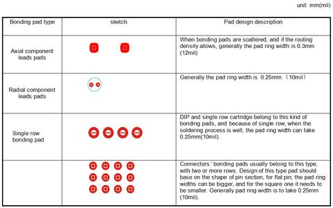
In consideration of soldering process, the bonding pads with cartridge components can be categorized into groups listed in Table 1.1, and recommended bonding pads size areseen in the content.

Table 1.1 Ring Width of Cartridge Components Bonding Pads Design
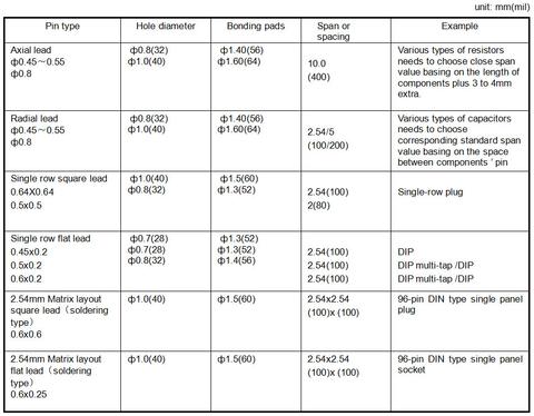
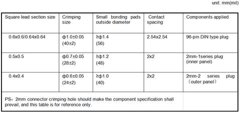
For the PCB with 1.6mm to 2mm panel thickness, the diameter of mounting hole and size of bonding pads of commonly used components are seen in Table 1.2 and 1.3.

Table 1.2 Bonding Pads and Hole Diameter of Commonly Used Cartridge Components

Table 1.3 Backboard Commonly Uses 2mm Connector Crimping Hole and Bonding Pads
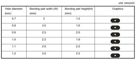
Commonly used elliptical bonding pads are shown in Table 1.4

Table 1.4 Commonly Used Elliptical Bonding Pads
Here you can find the second part of our Bonding Design post.