SMD component bonding pad design
2.1 Passive device pad design
2.1.1 Rectangle component pad design
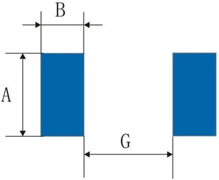
Shapes of resistor and capacitor and bonding pads are as shown in Figure 2.1.1. Bonding pads ’ width is calculated according to equation (1), resistor pad length is calculated by (2), and capacitor pad length is calculated by (3), and the space between pads is calculated by (4).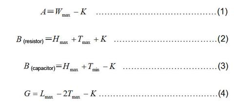 In the equations
A -- the height of bonding pad, mm(mil)
B -- the length of bonding pad, mm(mil)
G -- the gap length between pads, mm(mil)
W max -- the maximum width of component, mm(mil)
H max -- the maximum height of component, mm(mil)
T max -- the maximum width of component side bonding tip, mm(mil)
T min -- the minimum width of component side bonding tip, mm(mil)
L max -- the maximum length of component, mm(mil)
K=0.25mm (10mil)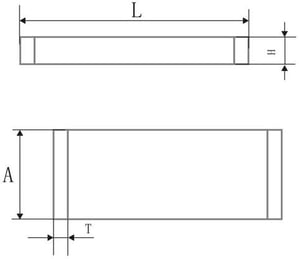
Commonly used bonding pads ’ size for resistor and capacitor are listed in Table 2.1.1(a) and Table 2.1.1(b).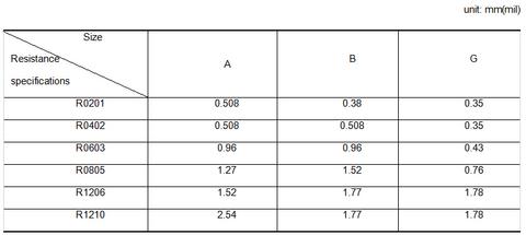
Table 2.1.1(a) Bonding Pad Size of Chip Resistor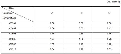
Table 2.1.1(b) Bonding Pad Size of Chip Capacitor
2.1.2 Molded plastic encapsulated tantalum capacitor pad design
Shapes of tantalum capacitor and bonding pad are seen in Figure 2.1.2. Bonding pads ’ width is calculated according to equation (5), length is according to (6), and gap is according to (7).  In the equations:
A -- the width of bonding pad, mm(mil)
B -- the length of bonding pad, mm(mil)
G -- gap length between pads, mm(mil)
W max -- the maximum width of component, mm(mil)
H max -- the maximum height of component (referring to the soldering side), mm(mil)
T min -- the minimum width of component side bonding tip, mm(mil)
L max -- the maximum length of component, mm(mil)
T max -- the maximum width of component side bonding tip, mm(mil)
K=0.25mm(10mil)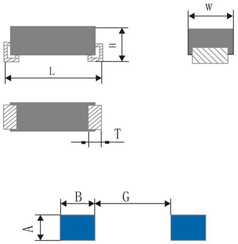 Figure 2.1.2 Shapes of Tantalum Capacitor and Bonding Pad
Commonly used molded plastic tantalum capacitor bonding pad sizes are listed in Table 2.1.2.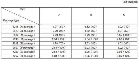
Table 2.1.2 Molded Plastic Tantalum Capacitor Bonding Pad Sizes
2.1.3 Cylindrical component bonding pad design
The shape of bonding pad is rectangle. When the reflow soldering process is applied, a concave groove must be designed (See Figure 2.1.3), and the width is usually 0.30.05mm. But if components are fixed by cementing compound before soldering, then there is no need to design a concave groove.
Commonly used cylindrical component bonding pad width, length, and gap, and length of concave groove are listed in Table 2.1.3.
Table 2.1.3 Cylindrical SMD Bonding Pad Size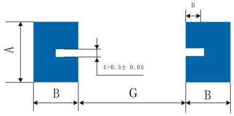 Figure 2.1.3 Cylindrical SMD Bonding Pad
2.2 Bonding pad design with devices
2.2.1 General rules
a) Width of bonding pad and pad distance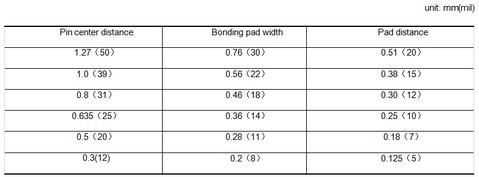
Table 2.2.1 Different Pin Center Distance with their Corresponding Bonding Pad Width and Pad Distance
b) Bonding pad length is 2.5 to 3 times of the solder PIN length, 3 times is recommended.
2.2.2. Transistor bonding pad graphic design
The center distance of bonding pad equals the center distance of leading wires. The size of bonding pad extend 0.38mm from around the soldering end (15mil). For most commonly used bonding pad SOT23、SOT89、SOT143, see Figure 2.2.2 (a), 2.2.2(b), 2.2.2(c).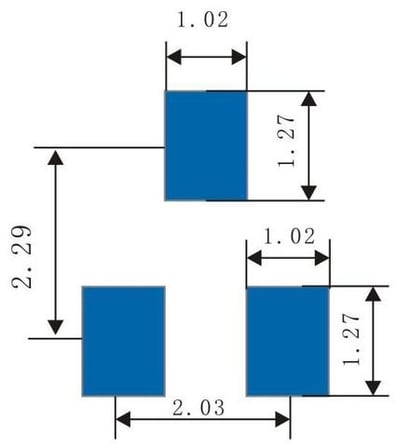
Figure 2.2.2(a) Sketch of SOT23 Bonding Pad (mm)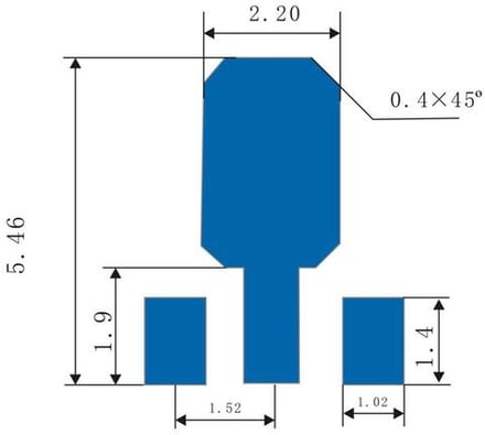
Figure 2.2.2(b) Sketch of SOT89 Bonding Pad (mm)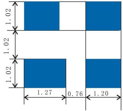
Figure 2.2.2(c) Sketch of SOT143 Bonding Pad (mm)
2.2.3 SOP Device bonding design
SOP shape and bonding pad shown by Figure 2.2.3, calculation of bonding pad width, distance between pads, bonding pad length by 2.2.1. Calculation of the inner flank distance of two rows bonding pad by equation (8).
In the equation:
D -- the relative distance of two sides bonding pad, mm (mil)
F -- the width of device, mm(mil)
K=0.254mm(10mil)
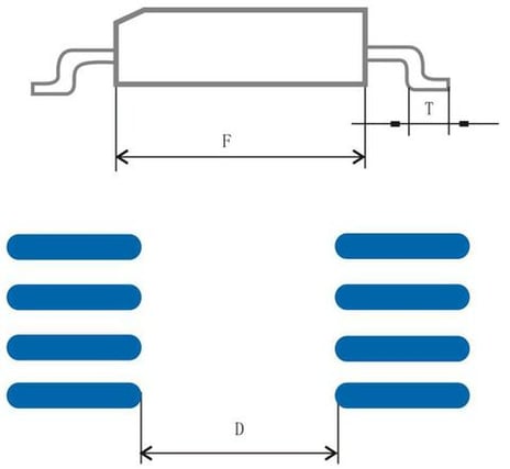
Figure 2.2.3 SOP Shape and Bonding Pad
2.2.4 PLCC devices bonding pad design
The shape of PLCC and bonding pad see Figure 2.2.4. Usually, the width of bonding pad is 0.76 mm, distance between pads is 0.51 mm, the length of pad is 2 mm, the equation (9) and (10) are for calculation of outer flank distance of boding pad.
In the equation:
A -- landscape orientation outer flank distance of boding pad, mm (mil)
B -- lengthwise outer flank distance of boding pad, mm (mil)
C1/C2 -- width of the device (include the pin), mm (mil)
K=0.76mm(30mil)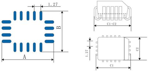
Figure 2.2.4 PLCC Shape and Bonding Pad
2.2.5 BGA and Ball grid array components bonding pad design rules
a). The center of every solder ball has to dovetail with the corresponding solder ball center at BGA bottom.
b). The pattern of PCB bonding pad is solid circle, through holes must not be made on the pad.
c). The width of conducting wires need to be same,in general 0.15mm~0.2mm.
d). Soldmask size has to be 0.1mm~0.15mm bigger than the bonding pad.
e). After though holes being punched and plated, block them with dielectric material and conductive adhesive, with its height should no taller than the bonding pad.
f). To process the screen graphics surrounding the four corners of BGA devices, line weight should be 0.2mm~0.25mm.
g). The bonding pad of BGA devices is round shape. Generally speaking, the diameter of bonding pad is 20% smaller than the solder ball’s. As for the pylomes beside the pad, soldmask need to be performed so as not to cause short circuit and cold solder joint by the loss of solder.
2.2.6 QFN (MLF、LLP and etc) type component bonding pad design
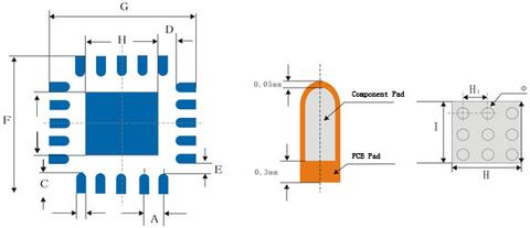
Figure 2.2.6 (a) and 2.2.6 (b)
Definition of QFN bonding pad:
A: Center distance of bonding pad
B: Width of bonding pad
C: Length of bonding pad
D: Minimum distance between function pad and thermal pad
E: Minimum distance between function pad and function pad
F、G:Maximum distance between function pads
H、I:Size of thermal pad
H1:Heat pad cooling vents distance
Φ:Diameter of vents (hole number decided by the size of grounding pads)
QFN bonding pad design parameter (see Table 2.2.6)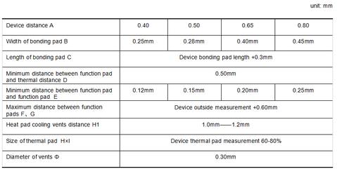
Table 2.2.6 QFN Bonding Pad Design Parameter
If you want to learn more about PCB design, we highly recommend you to check the following articles:
Posted by NexPCB United

Anything that was written as a group effort is added here. One for all, all for one!
