Before designing multi-layer PCB circuit boards, designers need to confirm the circuit boards structure primarily based on the scale of circuit, the size of circuit boards, and the requirements of electromagnetic compatibility (EMC).
The following table is the empirical data to determine number of signal layers based on the PIN density, for reference.

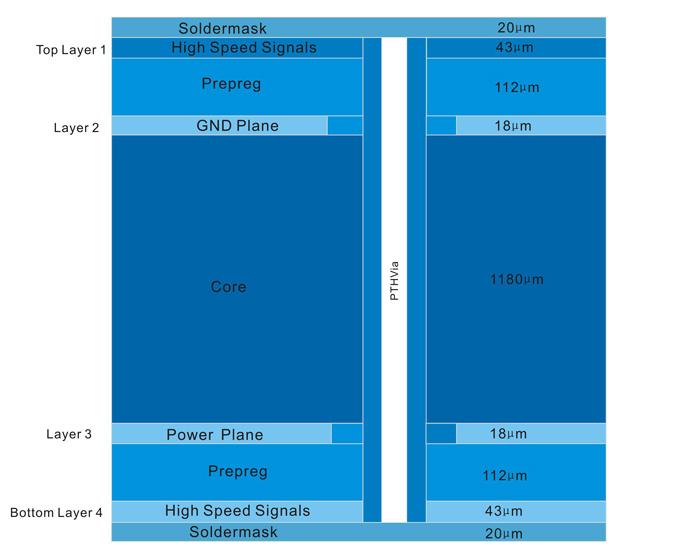
For your reference, a stack-up design for the four, six, and eight layered high speed digital signal PCB is demonstrated in below:
Four Layer Stack–Up
