1. Design of Through Hole
1.1 The design of through hole needs to meet the requirement that the hole diameter to the panel thickness ratio should be greater than 1/6.
1.2 Distance between holes.
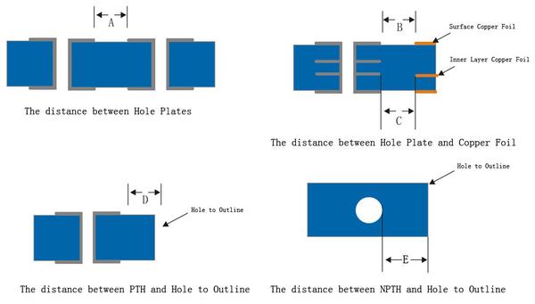
Figure 1.2 Distance between holes
PS: a). The distance between hole plates is: A≥20mil;
b). The distance between hole plate and copper foil is: B≥20mil, C≥20mil;
c). The minimum distance between PTH and hole to outline is the distance that can ensure the distance from the bonding pad to the hole to outline is: D≥20mil;
d). The recommended minimum distance between NPTH and hole to outline is E≥40mil.
1.3 The location of through hole is related with the reflowing soldering process.
The through holes cannot be designed on bonding pad, and they should be connected by a short printed line, the distance from hole wall to bonding pad must be greater than 0.2 mm, otherwise it is easier to produce flaws such as tombstone setting, useless soldering, and less tin, which is shown as follow:
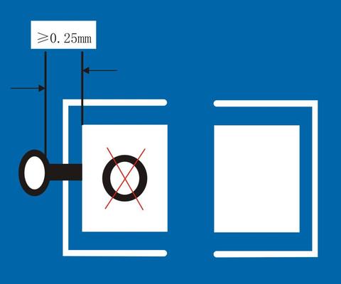
Figure 1.3 The Location Design of Through Hole
1.4 There should be no through holes in the extending outward 1.5 mm area of the contacting part of devices metal shell and PCB.
1.5 Through holes cannot be designed in the central area between two bonding pads that are on the chip component of the soldering face, see figure 1.5.
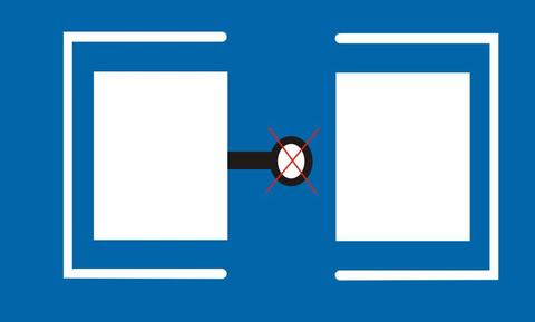
Figure 1.5 Incorrect Design of Through Hole Position
2. Locating Hole Design
2.1 Hole types selection

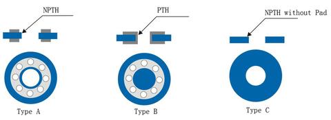
Figure 2.1 Types of Holes
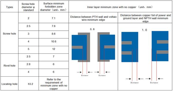
2.2 Design of forbidden zone
If you want to learn more about PCB design, we highly recommend you to check the following articles: