Voids in solder joints are a significant problem facing industrial products, especially in power electronics field. To achieve rapid and consistent heat conduction of power supply chip, it requires solder joints have a low and homogeneous thermal resistance. A closed cavity may cause path displacement of electricity or heat or local concentration of energy and heat. In addition, air cavities tend to be spherical during welding which may cause deviation of the component and the formation of wedge-shaped welding gaps. At the same time, it also makes the electrical current or heat uneven distribution worse, which cause stress and cracking of solder joints.
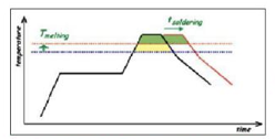
With the same material and same devices, solder joints may show a perfect performance on the surface, but the situation underneath is totally different. This is especially true when it comes to lead-free solder with a high melting point as it may need more reflow welding time to compensate for the high temperature limit.
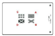
Similarly, the solder paste printing process has a great influence on voids rate. This is especially for devices (e.g. LGA) with planar terminal where the release of flux residues (chemical gas) causes a significant problem. One may think you could just overprint the area, but, from the point of view, there is no benefit in using the solder paste for the full area printing as it does not help to prevent voids. Different shapes of template openings have been tested in the manufacture of COB solder joints to see which has the best results. With X - RAY inspection and evaluation, type B printed graphics in the shape of an ‘X’ have been found to achieve the least amounts of voids. Because cross print solder paste graphics can make the solder flow from the inner directly to the outside in the welding process, it is not easy to form a closed space and voids, and is conducive to gas evacuation.
All current technology and applicable material can only limit the voids number and size but eliminating void on the overall is almost impossible. To completely eliminate voids, the most effective measures is using vacuum technology during soldering as the suction can remove most gases and flux residues from the solder joint. However, vacuum technology also has its own limitation as PCB material and some devices exhaust too much gas in the vacuum environment. This makes it difficult to reach a standard pressure and can slow down the process. There are also some electrolytic capacitors with sealed liquid, so these are also not suitable to vacuum technology. Another limitation is that in the vacuum, it is hard for convection heat transfer, usually only through infrared radiation or heat conduction, so can't fully heat the printed circuit board.
So to deal with this challenge, the best way to manage is to limit the potential for voids in solder by using the correct techniques for each individual product. Whether it’s using specially shaped solder paste printing or using vacuum technologies, a provider of these services needs to know the product well.
NexPCB can help with this process if you’re unsure. You can always contact us and our professional team of manufacturing engineers can help.
.png)


.png)