PCB Production
At PCB manufacturer NexPCB, one-stop service turning design into reality.
Services include Component sourcing, PCB layout, DFM, PCB fabrication, PCB assembly, Testing and Diagnosing.
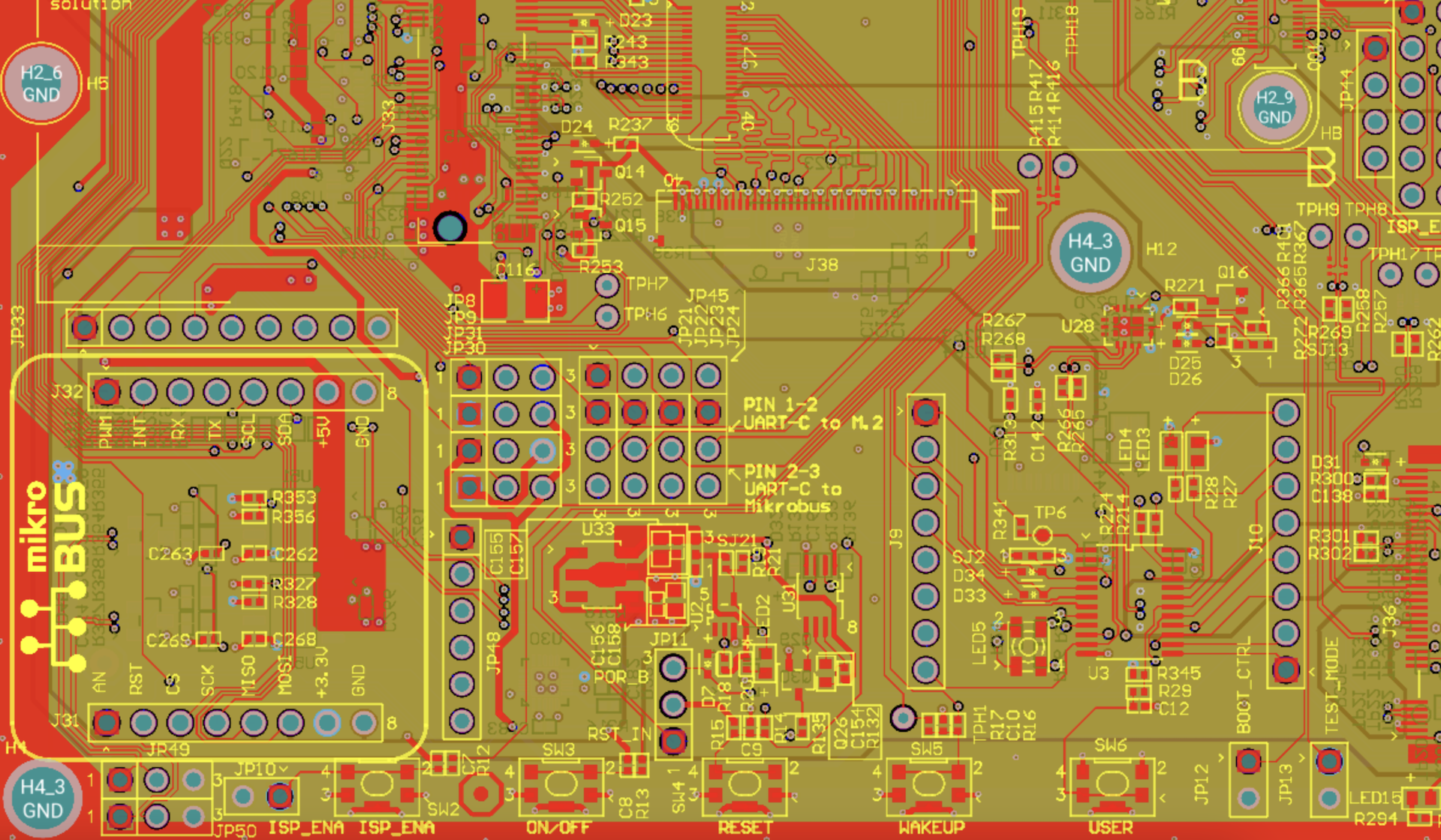
PCB Layout
Capable of creating up to 56 layers layout PCB, with tailored solutions for rapid, quality-driven deliveries.
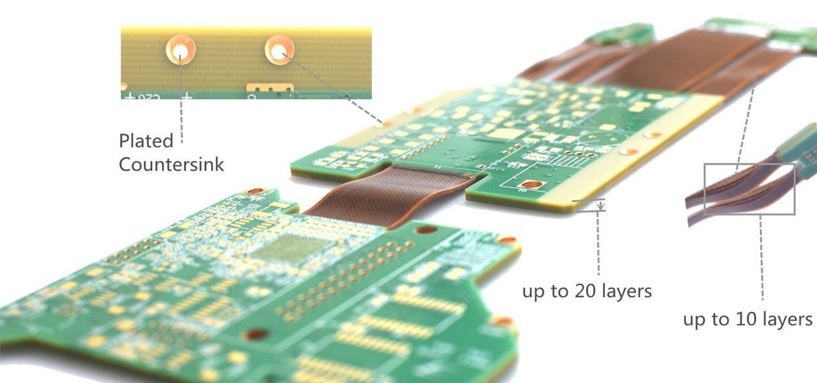
PCB Fabrication
Capable of creating up to 68 layers PCB. A standard minimum trace/space size at 3 mil. Advanced / HDI PCB also supported.
PCB Assembly
Precise connections for components like BGAs (pitch > 0.25mm). Tested with X-Ray checks.
Testing & Diagnosing
Collaborates and executes tests, RCA and documents results meticulously for the life of the product.
PCB Layout
| Standard | Advanced | |
|---|---|---|
| Layer Count | 24 | 68 |
| Max. Dimensions | 584mm x 508mm (±0.13mm) | 550mm x 900mm (±0.1mm) |
| Board Thickness | 0.2 ~ 3.2mm (±10%) | 0.1 - 10mm (±8%) |
| Copper weight (outer) | 1 - 5 oz | 1 - 18 oz |
| Copper Weight (inner) | 0.5 ~ 3 oz | 1/3 - 12 oz |
| Min Drill hole size | 8 mil | 6 mil |
| Min. Annular Ring | 4 mil | 3 mil |
| Min. Trace/Space | inner layer 3 mil, outer layer 4 mil | inner layer 2.5 mil, outer layer 3 mil |
| Min. Via | 8 mil | 6 mil |
| Min. BGA | 10 mil | 8 mil |
| Hole to hole clearance | 14 mil | 12 mil |
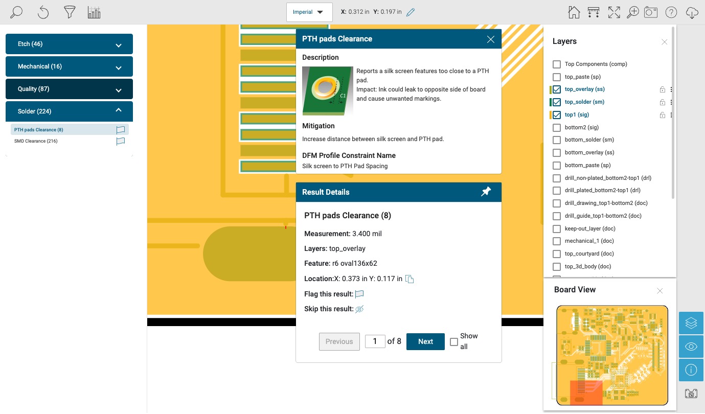
Design for Manufacturing
Seamless transition from design to production with reducing design iterations, costs and time-to-market.
Eligible experts working with industry tools, comply with the manufacturing constraints to review prior production to eliminate defects as earlier as possible.
Share your designs in various formats, including ODB++, IPC2581, Gerber274x.
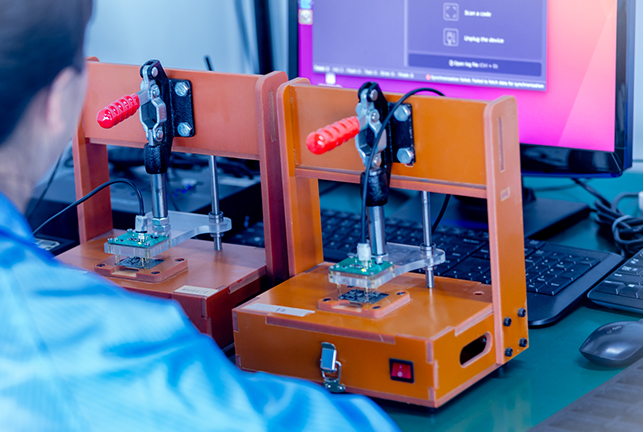
PCB Fabrication
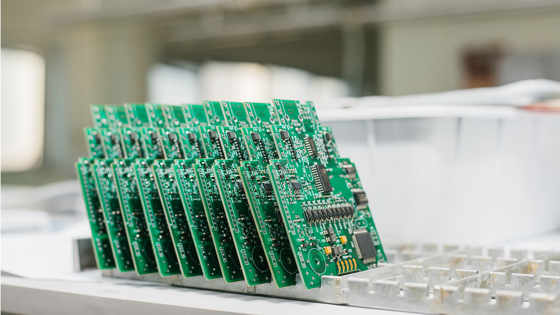
PCB Assembly
Wide range of PCB assembly capabilities with realiable lead time and high-quality delivery with any volume to keep your time promissing.
Supports Automatic Optical Inspection (AOI) and In-Circuit Test/Functional Test (ICT/FCT) for quality assurance. Covers soldering methods including reflow and wave soldering, precise connections for components such as BGAs pitch greater than 0.25mm. The smallest supported component size goes down to 01005 (0.2mm x 0.4mm).
Compliant with ISO 13485, IATF 16949 and ISO 9001. Acceptance criteria follows IPC standard demands.
Testing & Diagnosing
Our engineering team collaborates closely with customers to fulfill testing requirements, ensuring the execution of thorough testing protocols and delivering comprehensive test results prior to shipment.
Defect-related test results are meticulously documented and undergo a thorough analysis to identify root causes, thereby informing and enhancing our subsequent processes.
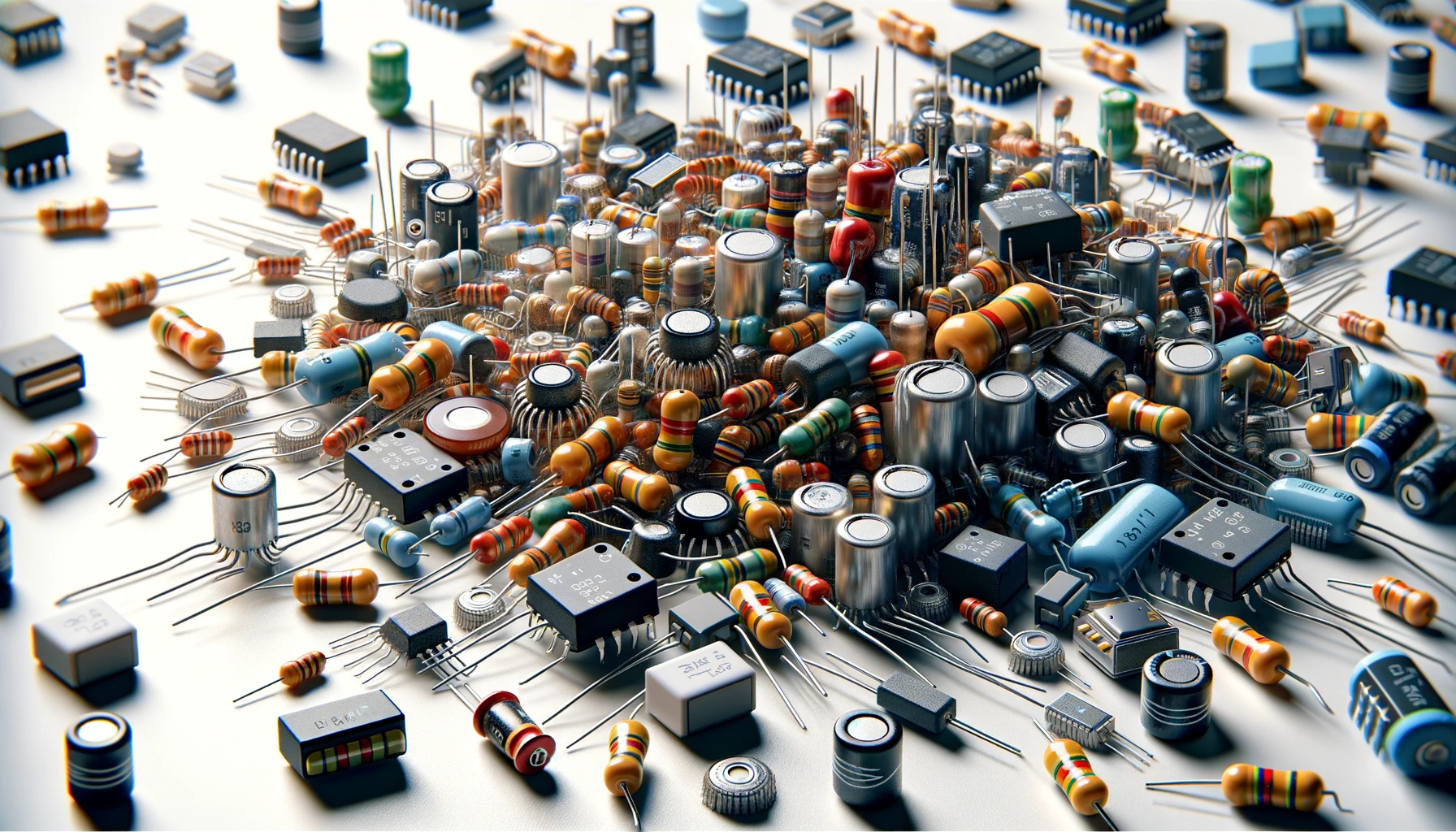
Component Sourcing
Engage directly with original manufacturers like NXP, TI, Murata, ST, Intel and etc, getting access to earlier emerging technology, and support throughout the design and prototype stages.
Moreover, our adept engineers excel in identifying alternatives during technical review, component shortages or end-of-life scenarios.