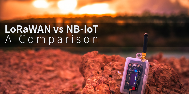
LoRaWAN vs NB-IoT: A Comparison
Aug 05, 2021 Detail
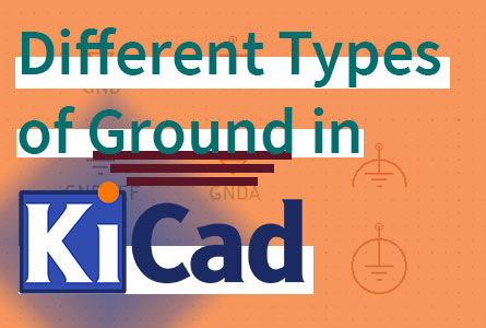
Different Types of Ground in KiCAD
Jul 19, 2021 Detail.jpg)
Pros and Cons of an Immersion Silver PCB Surface Finish
Immersion Silver, also known as IM silver, IMag, or ENIAg, among its other names, refers to the process of depositing a ...
Jun 10, 2021 Detail.jpg)
.png)