
Not all PCBs are manufactured the same way. Due to the processes that involve different chemicals, treatments, timelines, and heat levels, along with individual properties of PCBs like trace width, component density, placement methods, etc., different surface finishes may be required. Here is a list of common methods that we use to manufacture your PCBs.
Alternatively, you could also read our complete guide to PCB Surface Finishes in our Knowledge Base
Table of Contents
2) Organic Solderability Preservative (OSP)
3) Electroless Nickel+Immersion Gold (ENIG)
4) Electroless Nickel+Electroless Palladium+Immersion Gold (ENEPIG)
Hot-air Leveling (HASL)
Hot-air leveling Hot air leveling is the process of first coating the surface of the circuit board with lead-free tin solder, and then leveling it with heated compressed air to form a layer of copper oxide resistant coating on the surface. Although HASL delivers anti-oxidation at a cheap cost in a fast manner, surfaces formed using this method end up forming surfaces that are quite uneven due to the rough process. Make sure the solder being used doesn't contain lead in order to follow the RoHS compliance.
 Organic Solderability Preservative (OSP)
This is a method of surface plating in which an organic compound bonds over the bare copper surface. This layer provides similar qualities that the other surface finishes do. The process required to achieve OSP finish is fast and cost-effective. The downside is the difficulty to inspect due to its color transparency. If your goal is to protect exposed copper on your PCBs in mid-production, OSP might be the best choice out there. OSP can be used in conjunction with other technologies too, as it doesn't interact with gold surfaces.
Electroless Nickel+Immersion Gold (ENIG)
In this method, the nickel acts as a diffusion barrier to the copper, and the gold protects the nickel from oxidation. The nickel is in fact the layer where the soldering takes place. Apart from providing protection to the nickel layer, gold also has low contact resistance. ENIG is one of the most commonly used PCB surface finishes due to its high yield rate and adherence to the ROHS standards. If the process isn't controlled effectively, it may result in an unwanted phenomenon called black pad, in which the gold starts corroding the nickel and starts forming areas in the joint with a high phosphorus rate, especially when it comes to BGA pads. These reduce the rate of solderability immensely, causing opens that are realized at a much later stage in assembly, or even testing. ENIG plating thickness of each layer should be between 0.05 to 0.23 µm for the immersion gold layer and 2.5 to 5.0 µm for the electroless nickel. The thicker the immersion gold layer, the more likely it is to result in a black pad due to process complications.
⇑Back to top
Electroless Nickel+Electroless Palladium+Immersion Gold (ENEPIG)
As the name suggests, this is one of the most complicated surface finish methods for circuit boards. The electroless palladium layer in the middle prevents the formation of black pads. However, features such as unparalleled solderability, silver and aluminum wire bonding, and long shelf life come with a premium price and a longer lead time.
Hard Gold
Hard gold plating, as the name suggests, is hard. It provides far better friction resistance than its alternatives and is generally used to make [gold fingers]. So when you have a board that is designed to be inserted into another board like a RAM, you should go with the hard gold. It is important to mention that hard gold surfaces generally only exist on edge connectors and are not used for soldering purposes. Their purpose is to provide a robust surface against wear & tear.
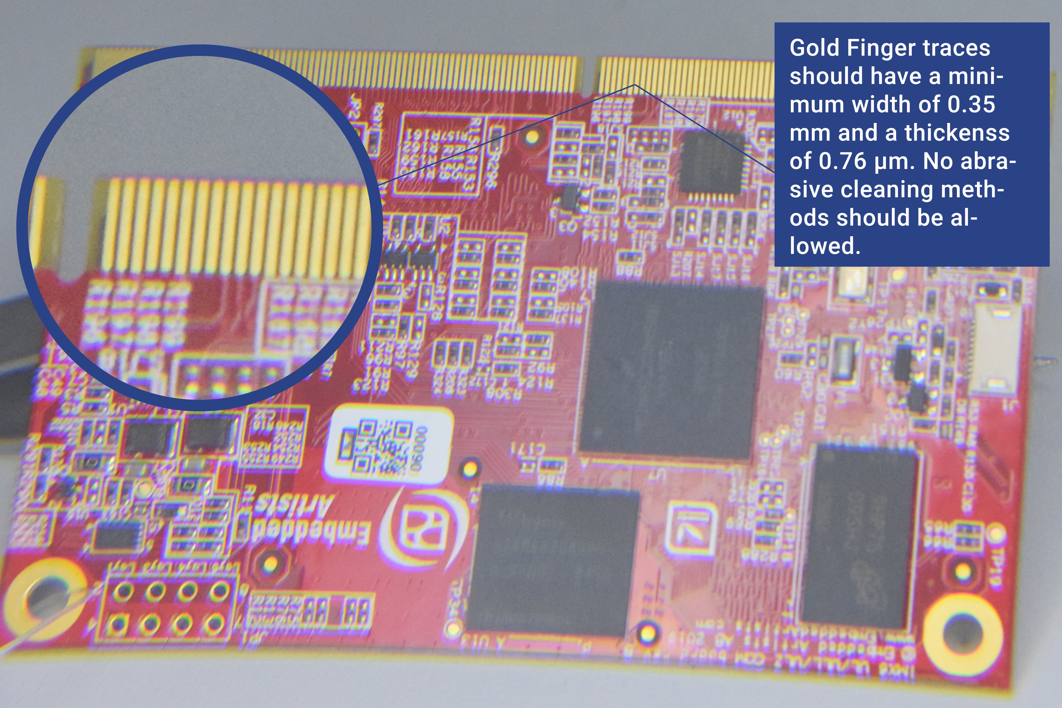
For both ENIG and Hard Gold techniques, we make sure that the thin gold surface finish is not damaged using highly abrasive or chemically active (surface is porous) cleaning methods. The alkaline cleaning agents we use remove any post-production debris that may be present on PCB surfaces like fingerprints, or dust.
⇑Back to top
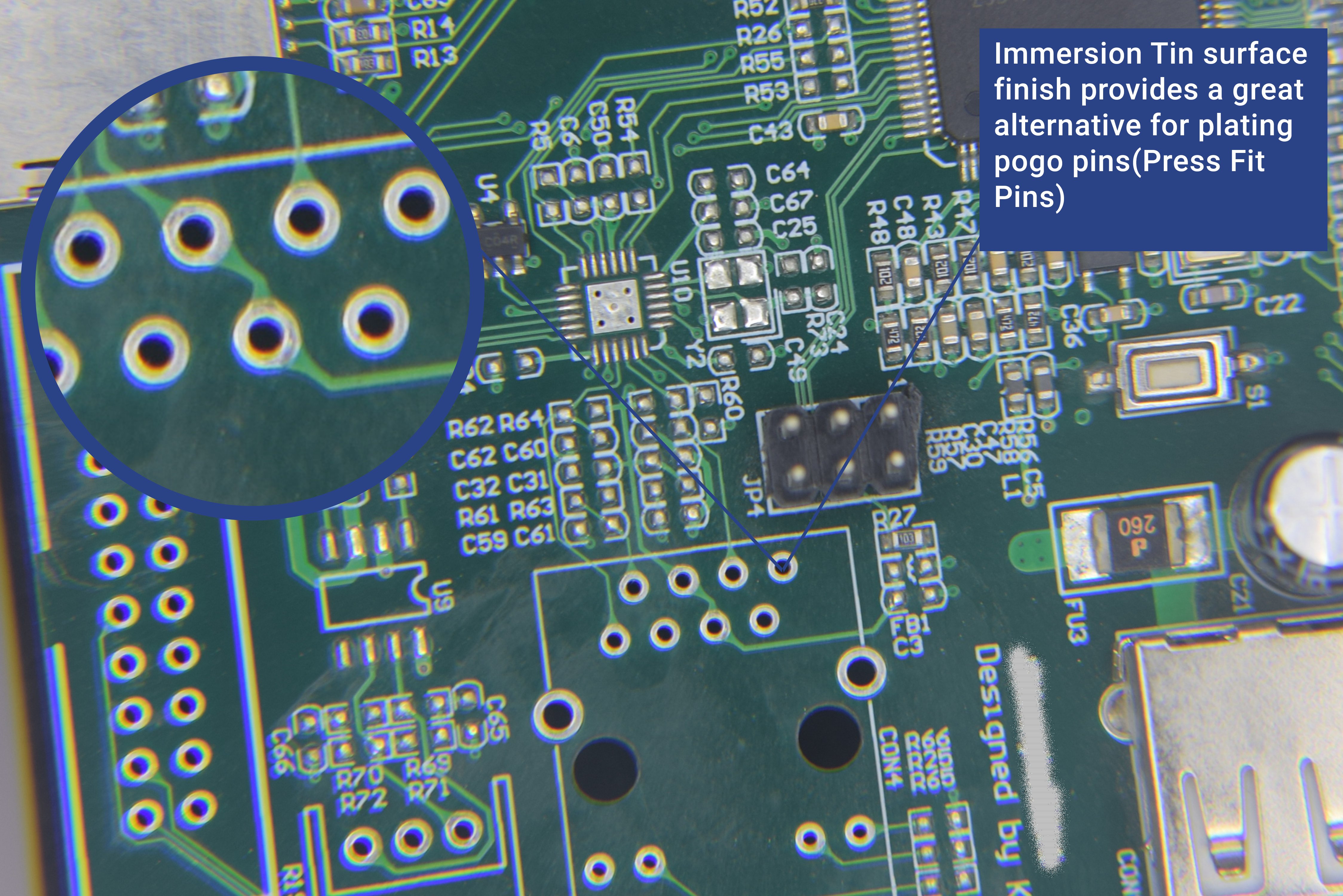
Immersion Tin
Some hate it, some just can't part with it, but it surely has been popular for a long time. Being a very well-researched process, immersion tin provides a flat surface that is 20-40 µin thick. Although it provides good solderability and is especially fit for pin insertion applications, it has some of the shortest shelf-lives at 3-6 months on average.
Immersion Silver
Although slightly more pricier than immersion tin, immersion silver finish provides everything that the aforementioned method provides at a thickness almost 4 times less than the former. On top of that, it provides better solder formation and is a great choice for boards with high-frequency signals.
As you can see, it is not right to claim that one method is better than the other one under all circumstances. Depending on what your board looks like, and what it intends to do, our DFM engineers can quickly assess your designs and make suggestions about what finish should be used.

bonus: Other Variables to Consider
Solder Flux Selection
Copper is easily oxidized in certain environments. Heat, humidity and salinity conditions can speed up the process of oxidation of copper. Older solder fluxes may also contain corrosive substances that may form shorts between nearby traces over time. This is usually not a problem with SMT as the temperatures will be sufficient to break down the acids. But when your boards require through-hole components, NexPCB ensures that the fluxes used will not have an adverse effect on the performance and the solderability of your boards.
Heat Intensity
Heat intensive methods such as HASL may cause deformation if the board thickness or material are not suitable. Heat levels of the process have to be tightly controlled to avoid damages to the solder mask too. Certain methods(such as immersion tin) may also cause more stress on the solder mask than others do.
If you found this post helpful, you should check out the following posts to learn more about PCB Design:
- Fundamental Technological Requirements of PCB Design
- Screen Printing Design
- How to create a PCB stencil File
- Panel Design
- Design of Hole
- Bonding Pad Design
- What is a Gerber file?

Orkun is the Marketing Manager at NexPCB. He's been living in China for almost 10 years. His passion lies in new and emerging technologies. You can contact him over LinkedIn for blog collaborations.